Blog

BLOG
Keep up to date with the latest news, information and updates from the Axelera team
- 42Items
- Home
- Blog
NewsApr 14, 2026
Voyager SDK: New Pipeline Builder and More
The latest version of Voyager® Software Development Kit (SDK) is here and this release touches nearly every layer of the stack. Whether you're deploying on new hardware, building custom inference pipelines, or are just tired of wrestling with installation scripts, there's something in this release for you.Release Highlights for version 1.6Top 3 highlights: Support for the new Axelera Metis® M.2 Max Install Voyager SDK with a single line of code Build complete inference pipelines in pure PythonAlso new in this release: New models added to the model zoo Track multiple objects with TrackTrack, including subjects that exit and re-enter the scene Optimize multi-camera pipelines for high-throughput, high-resolution inference Deploy Metis across more devices, OSes, and virtual environments Streamline your development workflow with improved toolsMetis M.2 Max: unprecedented performance in an M.2 form factorThe Metis M.2 Max provides an option from the Metis M.2 module, giving you double the memory bandwidth, a lower profile and advanced thermal management features for more demanding, but still compact, edge inference. This version of Voyager features support for the new Metis M.2 Max. The software takes full advantage of the module’s new capabilities to deliver the inference performance of a PCIe card, but in the compact M.2 form factor. This opens up deployment in space- and power-constrained edge devices such as retail kiosks, industrial gateways, and embedded vision systems without compromising performance.The increased memory bandwidth makes Metis M.2 Max particularly suited for running Large Language Models (LLMs) on edge devices. Additionally, the firmware implements closed-loop power control, letting you trade peak compute for a predictable power envelope. Set your limit with axdevice --set-power-limit and the hardware will make sure to stay within your thermal and electrical budget. When AI cores go idle, frequency drops automatically, saving roughly 0.6 Watts across all four cores with zero impact on active workloads.Install with pip, Run AnywhereThis is a big one for developer experience. The SDK is now delivered as standalone Python wheels which are installable via pip on Python 3.10 through 3.13. There are two wheels: axelera-rt for the runtime environment and axelera-devkit for the compilation/development environment.With ManyLinux compliance, these wheels work across multiple Linux distributions including Debian 12 & 13, RHEL 9 & 10, and Yocto-based distributions without needing the Axelera installer script. If you've been waiting to integrate Axelera hardware into your existing custom CI/CD or container workflows, this is your moment!Pipeline Builder API: a pythonic way to build inference pipelinesThe new Pipeline Builder API (currently in Alpha) lets you define entire inference pipelines, from model loading through post-processing and tracking, as composable Python expressions. You don’t need any YAML, or any additional boilerplate. You can chain operators with op.seq(), run branches in parallel with op.par(), and apply per-object processing with op.foreach().Example: Load a model, run inference, display detections, all in the same Python programming unitThe API ships with 30+ operators spanning pre-processing, inference, post-processing, filtering, and tracking. Results come back as typed objects (DetectedObject, PoseObject, SegmentedObject, TrackedObject) with .draw() visualization built in. A pipeline optimizer automatically fuses operator chains into SIMD-accelerated kernels where possible. The entire tensor layer is DLPack-compatible, so data moves zero-copy between the pipeline and PyTorch, JAX or NumPy without leaving device memory. Additionally, you can also package and export pipelines into the new packaging .axe portable format for easy redistribution.Expanded Model ZooVersion 1.6 adds significant coverage across vision tasks:Object Detection: GELAN-S/M/C (the Ultralytics YOLOv9 backbone), Ultralytics YOLO26-X, and the Ultralytics YOLO-NAS S/M/L family from Deci AI with quantization-aware blocks Instance Segmentation: Ultralytics YOLO26-N through Ultralytics YOLO26-X Seg variants Pose Estimation: Ultralytics YOLO26-N through Ultralytics YOLO26-X Pose Oriented Bounding Boxes: Ultralytics YOLO26 OBB variants for rotated object detection Re-Identification: SBS-S50 backbone enabling full Deep-OC-SORT re-identification tracking on Axelera hardwareAll new models ship with ready-to-use YAML pipeline files and pre-compiled downloads via axdownloadmodel.TrackTrack and Advanced Multi-Object TrackingThe tracking stack gets a major upgrade with TrackTrack, a state-of-the-art multi-object tracking algorithm from CVPR 2025 that uses iterative matching with track-aware NMS. It's implemented in C++ with Python bindings and available through both the YAML and Pipeline Builder APIs.Alongside TrackTrack, this release adds Camera Motion Compensation (CMC), which is critical for moving-camera deployments, for (Deep-)OC-SORT and an experimental Memory Bank feature that lets the tracker restore a person's ID after they leave and re-enter the scene.Multi-Stream Tiling and OpenCL AccelerationFor multi-camera deployments, tiling pipelines now support multiple camera sources simultaneously, with per-stream tiling configurations via the tile[...]:source syntax. New tools (tile_config.py, camera_scan.py) automate pipeline generation and camera setup.On the performance side, face alignment, color conversion, polar transforms, and region of interest cropping are now OpenCL-accelerated, and DMA buffer passthrough on ARM eliminates memory copies, particularly valuable on the Metis Compute Board where camera and display share DMA buffers.Broader Platform and Virtualization SupportBeyond the new operating system support already mentioned, version 1.6 adds:Yocto integration via meta-axelera and build sources for the Metis Compute Board KVM PCIe passthrough (currently in Beta) to pass Metis devices into VMs with the full runtime stack running inside the guest New validated hardware platforms including the Dell Pro Slim Plus XE5 and AsRock NUC Box-125 PyTorch 2.7–2.10 support in the compilation environmentDeveloper Tooling ImprovementsAs we continue to improve the developer experience and tooling, the following updates were made:TOML compiler configs replace JSON as the default as they are more readable and more editable (JSON still works if you prefer it.) axcompile is the new CLI entry point, replacing python -m axelera.compiler.compile axdownloadmedia fetches test videos and images from cloud storage for benchmarking and experimentation axdevice driver --install automates PCIe driver setup on Debian systems axmonitor now shows DDR bandwidth plots and extended power measurements, making it easier to identify whether workloads are memory-bound or compute-bound The PCIe Linux driver source is publicly available under a GPLv2 license, so you can build the kernel module yourselfTry it outVoyager SDK v1.6 is available now: # Installation (on Linux)git clone https://github.com/axelera-ai-hub/voyager-sdk.gitcd voyager-sdk./install.sh --all --YES --media# Run a Computer Vision application using Yolov8axdownloadmodel yolov8l-coco./inference.py yolov8l-coco media/traffic1_1080p.mp4# Run an LLM chatbot using Llama3.2axllm llama-3-2-1b-1024-4core-static --prompt "Tell me a joke"For the full release notes, documentation, and technical support, visit the Axelera AI Customer Portal.We'd love to hear what you build with it! Comment below or share more about your project in Axelera’s Community.
Related products:AI Software
TutorialApr 14, 2026
The Voyager Pipeline Builder API: Inference Pipelines as Python Expressions
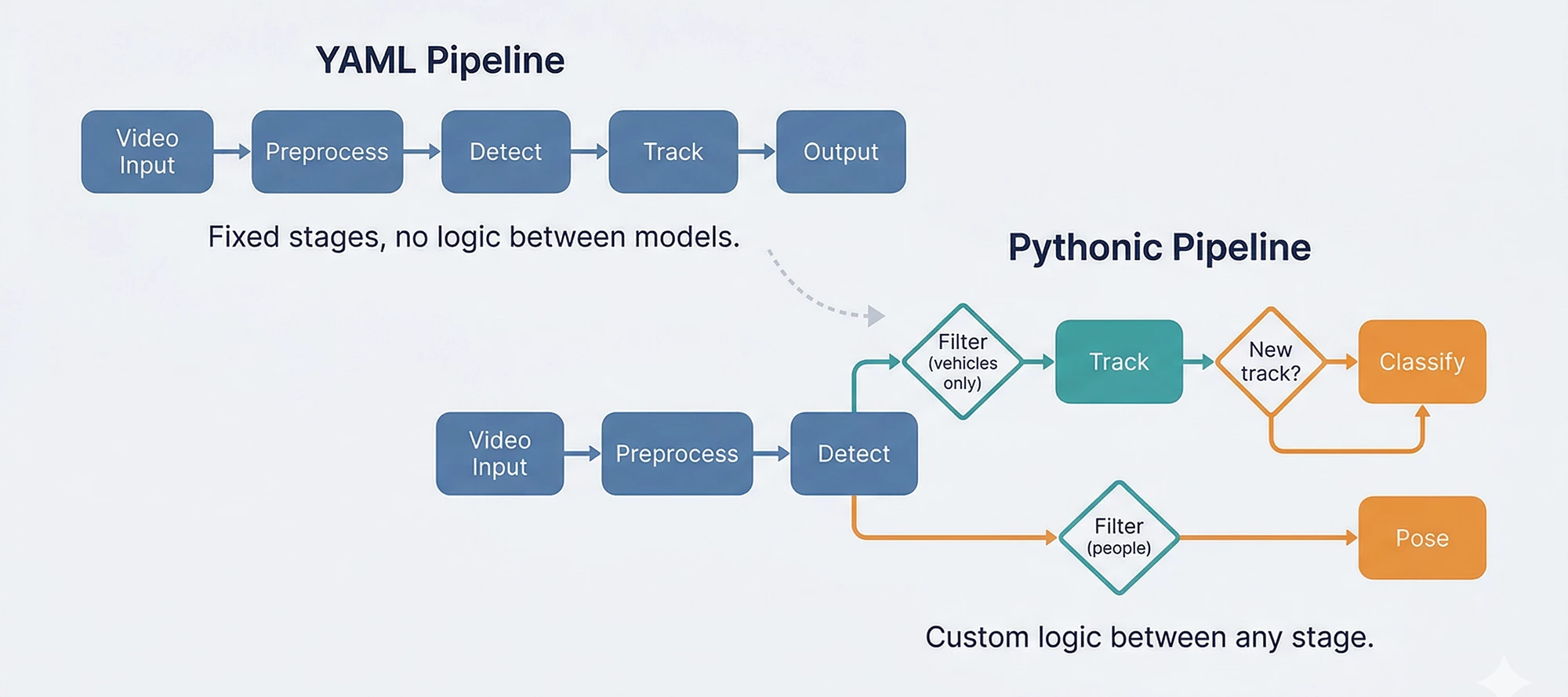
We made a deliberate bet when we built the Voyager® Software Development Kit's (SDK) pipeline builder: YAML-described pipelines, not code. A single YAML file would define everything from video input to model inference to postprocessing. The SDK would handle GStreamer orchestration, multi-stream management, image preprocessing like camera distortion correction, color conversion, and hardware dispatch. Application engineers could deploy detection and tracking pipelines without writing inference code at all.That bet paid off. Production security systems, traffic analytics, and retail deployments run on YAML pipelines today. A detection-with-tracking pipeline looks like this:pipeline: - detections: model_name: yolo26s preprocess: - letterbox: width: 640 height: 640 - torch-totensor: postprocess: - decodeyolo10: conf_threshold: 0.4 - tracker: model_name: oc_sort cv_process: - tracker: algorithm: oc-sort bbox_task_name: detectionsAnd the application code to consume it:stream = create_inference_stream(network="yolo26s-coco-tracker", sources=["camera.mp4"])for frame_result in stream: for obj in frame_result.tracker: print(f"{obj.label.name} {obj.track_id}")The approach is compact, declarative, and fast. For standard detect-and-track workflows, this delivered on two of the three things edge AI developers need: performance and ease of use. The third, flexibility, is where the story gets interesting.Then users started building things we didn't plan forA customer needed to detect vehicles, track them, and run a secondary classifier only on newly appeared tracks entering a specific zone. Another wanted to split detections by class, run different models on each subset, and merge the results with custom business logic. A third wanted to prototype cascade pipelines in a Jupyter notebook before deploying to production.The YAML pipeline can support all of these, and we have customers in production using such capabilities, but each new inter-stage pattern requires C++ and Python development to enable it. YAML cascades work through predefined reference patterns (source: roi, where: task_name) that connect stages together declaratively. Adding custom logic between stages, such as: "only classify if the track is new" or "skip this model if the confidence is below X and the object is in zone B," means building new C++ components and Python wrappers for each specific case. Voyager’s foundational runtime objects (InferenceStream and AxInferenceNet) are extensible to support inter-stage, but the development cost scales with every new pattern.There was also a subtler friction: ML engineers prototype in PyTorch and NumPy. They think in tensors and function calls, not YAML keys. Asking them to translate a working Python prototype into YAML configuration added a step that slowed iteration without adding value.The YAML abstraction was right for deployment. It wasn't fast enough for development iteration.In YAML, custom logic between stages requires C++ and Python development. The Pythonic builder puts it in your hands.What if the pipeline IS the code?That question led to the Pythonic Pipeline Builder — an experimental API where pipelines are composed in Python, not described in YAML. The same detection pipeline, in code:from axelera.runtime import oppipeline = op.seq( op.letterbox(640, 640), op.totensor(), op.load('yolov8n-coco.axm'), op.decode_detections(algo='yolov8', num_classes=80), op.nms(), op.to_image_space(), op.axdetection(class_id_type=op.CocoClasses),)detections = pipeline(image)Each operator does one thing. op.seq chains them. The pipeline is a callable. This isn't a wrapper around the YAML system; it's a separate runtime that gives direct access to the same optimized C/C++ operators, with the flexibility to compose them however the use case requires.But the real point isn't the detection pipeline. That works fine in YAML too. The point is what happens when you need to go beyond it.The moment it pays offHere's the vehicle-tracking scenario in Python. Detect vehicles, filter by class, track them, classify only newly appeared tracks. The kind of inter-stage logic that would normally require dedicated C++ development:from axelera.runtime import opdetect = op.seq( op.colorconvert('BGR', 'RGB'), op.letterbox(640, 640), op.totensor(), op.load('yolov8n-coco.axm'), op.decode_detections(algo='yolov8', num_classes=80), op.nms(), op.to_image_space(), op.axdetection(class_id_type=op.CocoClasses), op.filter(class_ids=[op.CocoClasses.car, op.CocoClasses.truck, op.CocoClasses.bus]),)tracker = op.tracker(algo='bytetrack', return_all_states=True)classify = op.seq( op.croproi(property='bbox'), op.resize(size=256, half_pixel_centers=True), op.centercrop((224, 224)), op.totensor(), op.normalize(mean=[0.485, 0.456, 0.406], std=[0.229, 0.224, 0.225]), op.load('vehicle-type-classifier.axm'), op.axclassification(), op.topk(k=1),)for frame in video: with op.frame_context(frame): detections = detect(frame) tracked = tracker(detections) for obj in tracked: if obj.state.name == 'new': label = classify(frame, obj.tracked) print(f"New vehicle {obj.track_id}: {label}")The filter, tracker, and classifier are separate pieces that compose freely. The "only classify new tracks" logic is a Python if statement, not a C++ component, callback library, or feature request. When the business rule changes (classify lost tracks too, or skip trucks, or add a second classifier for color), the change is a line of Python, not a development cycle.You don't have to choose oneDuring this experimental period, the most practical path for many teams is a hybrid: keep YAML for what it already does well, and hand off to Python where flexibility matters.Concretely: a YAML pipeline defines the top-level models (detection, pose, segmentation) without cascading. InferenceStream handles video acquisition, image preprocessing, multi-stream management, and primary inference at full GStreamer-optimized throughput. Then in your application code, Pythonic operators take the detection results and run tracking, filtering, secondary models, and business logic, all in Python.This isn't a migration. It's a bridge. Teams keep their existing YAML pipelines and add Python where the development cost of enabling new patterns in YAML outweighs writing them directly. As the Pythonic builder matures, more of the pipeline can shift over incrementally.What's ready and what's notThe experimental version of the Pythonic Pipeline Builder ships with Voyager SDK 1.6. We want to be clear about where it stands.What works today: The operator API (op.seq, op.filter, op.tracker, op.foreach, custom operators), detection/classification/pose/segmentation pipelines, and four tracking algorithms. Models compile through the Ultralytics integration or the compiler API for any ONNX/PyTorch model. Getting started and pipeline overview docs ship with the SDK.What's not ready yet: The optimized fused kernels that give YAML pipelines their peak throughput haven't been ported to the Pythonic builder yet. Each release will close this gap. The YAML and Pythonic paths also use different model compilation workflows today. The next beta will unify these so a model compiled once works with both. And a new video orchestration system is in development to replace the GStreamer dependency with something more flexible.The goal has always been all three: performance, ease of use, and flexibility. The YAML builder delivered the first two. The Pythonic builder is how we add the third, without giving up what already works.Which way do you lean?This direction is shaped by how developers actually use the SDK. Do you prefer YAML for its simplicity? Is the Pythonic API closer to how you think about pipelines? Would a hybrid fit your workflow best?Let us know in the comments. Your input directly shapes what we build next.
Related products:AI Software

BlogApr 8, 2026
Run Ultralytics YOLO on Axelera AIPUs in Minutes
Trying new AI hardware typically means weeks of integration work before you can tell if the hardware is even worth it. There’s a new compiler, new runtime, and new preprocessing quirks. By the time you've ported your model and built the surrounding pipeline, you've invested a quarter and still don't know if the accuracy holds up.The Ultralytics and Axelera® AI integration removes that barrier. If you train with Ultralytics, you can export to Axelera’s Metis® AIPU, validate accuracy, and run a working application, all without leaving the tools you already know. Once you’re running on Metis with the Voyager® SDK, you can tap into the high performance and low power needed to solve your edge AI inferencing challenges. With four independently programmable cores, you can run models in parallel, easily build an end-to-end pipeline, implement adaptive tiling for high resolution inference, and scale your hardware without reworking your pipeline configuration. Export: One Commandfrom ultralytics import YOLOmodel = YOLO("yolo26n.pt")model.export(format="axelera")That's it. The export compiles and quantizes your model to int8, producing an .axm file optimized for the Metis AIPU. No retraining. No architecture changes. No hardware expertise required to get started.The integration supports detection, pose estimation, instance segmentation, oriented bounding box (OBB), and image classification across Ultralytics YOLOv8, Ultralytics YOLO11, and Ultralytics YOLO26 models. If you've trained it with Ultralytics, it exports.Validate: Know Before You CommitAccuracy is the first question every machine learning (ML) engineer asks when evaluating new hardware, especially hardware that quantizes to int8. And historically, answering that question has been painful. Most vendors publish model zoo benchmarks, but those benchmarks use the vendor's own validation pipeline, which may not match your training framework's baseline. The comparison isn't apple-to-apple. And it's not your model; it's a reference model with reference weights. You still don't know if your specific model retains accuracy on that hardware.The Ultralytics integration changes this. You validate with the same yolo val you already trust:yolo val model=yolo26n_axelera_model data=coco.yamlyolo predict model=yolo26n_axelera_model source=test_image.jpgTwo checks, both using tools you already know:Quantitative: yolo val runs your validation or test set and gives you mAP numbers for the Metis-compiled int8 model compared directly against the same baseline you trained with. No separate tooling is required and it doesn’t use proxy benchmarks. Qualitative: yolo predict runs inference on your own test images so you can visually inspect the results. Does it look right on your data?Metis is designed for high-accuracy int8 inference. The hardware and compiler use mixed-precision techniques under the hood to preserve accuracy where it matters most, while keeping int8 throughput. You can verify the results yourself in minutes rather than taking our word for it.The takeaway: you can evaluate the Metis AIPU for your use case in an afternoon instead of a quarter. If the accuracy numbers work, then keep going. If they don't, you've lost hours, not months and you can focus on optimizing for your use case.Build: From Export to ApplicationYou have a compiled model. Now how much code does it take to build a real application around it?This is one of the hello-world examples that ship with Ultralytics. It includes pose estimation with multi-object tracking, and it’s ready to run:from axelera.runtime import oppipeline = op.seq( op.colorconvert("RGB", src="BGR"), op.letterbox(640, 640), op.totensor(), op.load("yolo26n-pose.axm"), ConfidenceFilter(threshold=0.25), op.to_image_space(keypoint_cols=range(6, 57, 3)), op.tracker(algo="tracktrack"),).optimized()for frame in video: tracked_poses = pipeline(frame) for pose in tracked_poses: draw_skeleton(frame, pose)That's the entire pipeline: preprocessing, inference, postprocessing, and tracking in just 15 lines of Python. You don't need to be a deployment expert. Voyager SDK's Pythonic pipeline builder handles the low-level orchestration, so all you need to do is describe what happens at each stage.For production, the pipeline builder runtime (axelera-rt) is lightweight. It doesn’t require PyTorch, CUDA, or a heavy ML training stack. It has the runtime your application needs for edge AI. When you move from evaluation to deployment, you drop the training dependencies entirely.Voyager SDK includes both a YAML-based pipeline builder for production deployments and this newer Python API. The Python path is the natural fit for ML engineers coming from Ultralytics because it reads like the model pipeline you would sketch on a whiteboard.Each operator does one thing:op.seq chains them .optimized() fuses adjacent operations for speed the tracker adds persistent identity across frames (switch algorithms by changing a string) ConfidenceFilter is a custom operator (you subclass op.Operator, and then write a __call__ method).The pipeline isn't a black box, so you can insert your own logic anywhere in the chain.What Production Looks Like at ScaleThe same pipeline patterns you just saw scale far beyond a single camera.At ISC West 2026, we ran a live demo processing two 8K camera feeds and one 4K feed simultaneously on three Metis 4-chip PCIe cards. The system ran 48 parallel model instances covering person detection, pose estimation, face recognition, weapon detection, and PPE identification, all in real time.This is a developer blueprint for what production edge AI looks like at scale. It runs on the same Voyager SDK and Metis AIPUs available today. The hardware scales from a single-chip M.2 module to a four-chip PCIe card, but your pipeline code stays the same. When Axelera's next-generation Europa AIPU ships, it runs on the same SDK.Read the full technical breakdown in the ISC West 2026 blog post.Why Metis Is Built for ThisRunning demanding workloads at the edge requires hardware engineered for exactly that. Metis is built on Digital In-Memory Compute (D-IMC) architecture, which brings computation directly to where the data lives rather than moving data to a separate compute unit. The result is more performance per watt, which matters when you are deploying to edge environments where power budgets are real constraints. Four independently programmable cores give you the flexibility to run four different models in parallel, or to mix and match single-model and cascaded configurations depending on what your application needs.Voyager SDK is designed to meet you where you are: a clean Python API and YAML pipeline builder for straightforward deployments, and lower-level access for developers who want to go deeper. Features like adaptive tiling let you run accurate inference across multiple 8K video streams without retraining your models. The same SDK that runs on a compact M.2 module scales to enterprise and edge server deployments without changing your pipeline code.One platform. Infinite possibilities.Get Started Follow the Ultralytics Axelera integration guide for setup (firmware, SDK installation, export, and validation) Run the hello-world examples (pose tracking and instance segmentation, ready out of the box) Explore the Voyager SDK on GitHub for the full model zoo, pipeline examples, and documentationTell us what you're building. We'd love to hear in the comments.
Related products:AI SoftwareAI AcceleratorsAxelera Community
BlogMar 31, 2026
Scaling Edge AI for the Enterprise: Building the Ultimate Multi-Model, Multi-Stream Security System
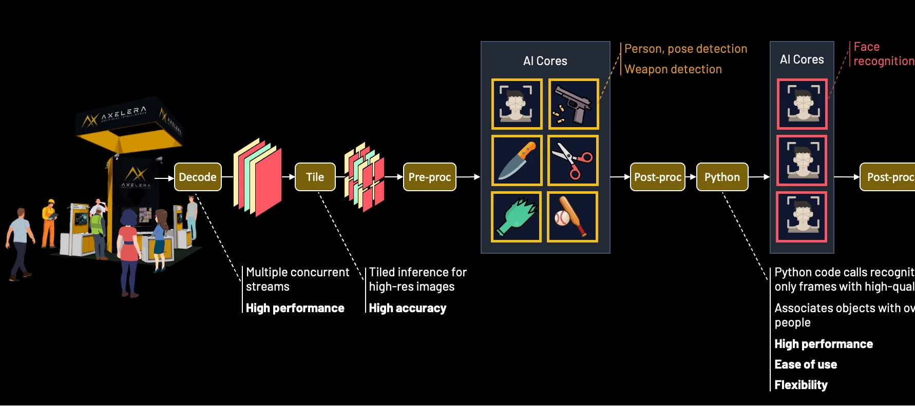
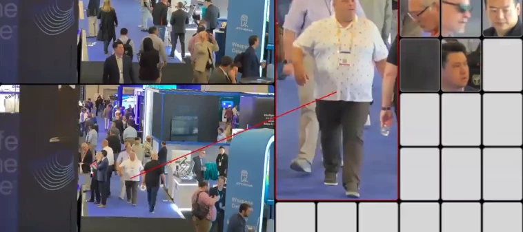
This piece covers the how. If you want the why, our companion article makes the business case for edge AI in physical security.At a Glance The Achievement: Real-time AI person-of-interest (POI) identification and threat detection across multiple 8K streams at 2.5 PetaOPS The Stack: Voyager SDK + Axelera Metis + Intel Xeon The Future: 3x performance leap with the next-gen Europa architecture Nothing matches the energy of ISC West for showcasing what we’ve been building. As we move between major industry events, we’re constantly hearing from enterprise leaders that the 'pilot phase' of Edge AI is truly over. The challenge now is scale. It’s no longer about running a single model on a single stream. It’s about the massive task of orchestrating dozens of AI models across multiple video feeds at commercially viable costs.Returning to this show in 2026 with our most ambitious interactive experience yet, is a turning point. It provides the perfect backdrop to demonstrate exactly how we’re pushing the limits of real-time, multi-model, and high-resolution multi-stream security.Last year we demonstrated a pioneering approach to 8k AI inferencing. Today, we’re expanding the Voyager SDK with safety-focused capabilities, including person-of-interest identification and an alerting and visualisation framework. These tools are designed to improve operator response times, particularly when potential weapons are detected on the show floor. In collaboration with four ISV partners, we’ve developed a security demonstration showing how easily customers can train, deploy, and integrate custom models into our end-to-end software pipelines to deliver plug-and-play AI solutions at scale. This showcase highlights the maturity of the Voyager SDK.If you are ready to build something like this yourself, here is where it gets interesting.Production Pipelines for Scalable Real-World SystemsWhen you build on Axelera's Metis AIPUs and the Voyager SDK, you gain a complete set of capabilities for orchestrating high-concurrency, multi-stream AI workloads out of the box. Here is what developers can tap into: Hardware-accelerated decoding: Ingest and decode multiple 4K and 8K video streams simultaneously to maintain low latency and high throughput Tiling-based pre-processing: Subdivide high-resolution streams into overlapping tiles to ensure the AI detects small objects with high precision, while applying perspective transformations to normalize different camera angles Concurrent analytics: Run multiple models in parallel to detect and track individuals, face landmarks, and objects of interest simultaneously Model cascading: Pass detector outputs to secondary models; for example, output regions of interest from a face detector to a recognition model Custom pipeline logic: Integrate user-defined code; for example, implement conditional logic to select specific frames or regions of interest to pass to secondary models Intelligent edge orchestration: Optimise bandwidth by sending only critical metadata/events to the cloud while retaining raw high-resolution footage for local forensic storage New to the Voyager SDKSupport for custom C++ and Python logic within the pipeline, providing the architectural flexibility demanded by modern, high-performance applications.Security person-of-interest pipelineReal-Time Person-of-Interest IdentificationThe ChallengeReal-world environments are far from ideal for identifying and tracking people of interest. The subject moves through crowds and around objects that obscure the view of them and they may actively avoid cameras, looking away or moving through dense crowds. Systems must also contend with challenging conditions such as poor lighting, motion blur, and varied facial angles.Facial recognition models are highly sensitive to the quality of input. Indiscriminately processing blurry, angled, or partially occluded faces increases false rejections (failing to identify a known subject) and false identifications (incorrect matches), all while wasting valuable AI processing cycles.The SolutionA shift is necessary from frame-by-frame recognition to more nuanced temporal processing. By inserting a tracker after the detector, developers can identify the same individual across multiple frames and construct a pose-quality buffer for each tracker ID. Combined with conditional logic, this allows the system to filter for only the highest-quality detector crops, preserving processing power while improving accuracy.As a tracked person moves through a scene, their associated pose-quality buffer is populated with the best available regions of interest based on metrics such as pose angle, pixel density, and illumination. Each new region of interest replaces the weakest frame in the buffer only if its score is higher. Over time, poor angles and blurs are filtered out, ensuring only the most reliable data reaches the recognition model.Anchor and UpdateThe first high-quality region of interest detected can be immediately cascaded to the recognition model, allowing the system to make a primary identification while the pose-quality buffer populates. Once the buffer reaches a defined threshold, the system performs batch processing to refine the result. Instead of treating each match in isolation, the recognition outputs are combined using a Bayesian update to produce a cumulative confidence score. This effectively amplifies multiple lower-confidence matches into a single, high-certainty identification.This process treats each new region of interest as a multiplier of existing evidence. Mathematically, two independent 70% matches provide greater certainty than a single 90% match. This architecture ensures temporal stability and resilience against noise or outliers. Once a high-confidence identity is established through multiple high-quality frames, transient data from a blurry frame or passing occlusion will not overturn the cumulative evidence.Secure the Critical MomentAn override gate ensures that the system identifies subjects who may only appear clearly for a single frame. If an incoming region of interest achieves a high-quality frontal pose and returns a high-confidence match, the identification is considered immediately reliable. This triggers an instant alert and can be configured to supersede the existing buffer of lower-quality data. This mechanism prevents temporal blindness by ensuring that even a fleeting, high-quality glimpse of a subject results in a successful identification.Region-of-interest (ROI) processingThe Axelera Surveillance BlueprintNext, we put the person-of-interest tracker together with real-time weapon detection, designed specifically for multi-model concurrency. This blueprint allows developers to easily extend the system by running a range of analytics models in parallel.To maximise detection reliability, each subject is represented as a detection pair: person and face. By running person and face detection models in parallel on every frame, the system maintains dual-path tracking: faces can be identified even when bodies are occluded by crowds or objects, while individuals can be tracked when their face is not visible. The application dynamically maps overlapping detections to maintain a persistent identity for each subject.The pipeline is configured to prevent frame-drop: if a new frame arrives before all recognition tasks complete, the remaining tasks are asynchronously scheduled across subsequent detections. This allows the system to iteratively scan and resolve an entire scene over time without compromising camera throughput (similar to how a human would process the scene, just much faster).The blueprint is engineered to commit fast and refine slow. It uses the first high-quality match to establish an initial identity with low latency, while maintaining a pose-quality buffer to improve certainty over time. Combined with the override gate, this ensures that even brief, high-quality captures result in a successful identification.To manage these detections, the interface displays all tracked individuals in a grid of high-resolution regions of interest, a crowd view. Utilising the full 33-million-pixel resolution, this enables operators to maintain visibility on distant subjects that would otherwise be lost to downscaling on most monitors. The interface uses bi-directional linking: when you hover over a person in the grid, the system draws a line to their position in the raw feed, and vice versa. At a single toggle, the grid can be configured to show the live view of each person or the best shot from the pose quality buffer.Combined person-of-interest tracking with weapon detectionWeapon DetectionWhile I’d have loved to show a realistic weapon demo, the venue (and the common sense of my colleagues) suggested that bringing firearms onto the show floor was a bad idea. Instead, I opted for a weapon from a more civilised age: a lightsaber.For the weapon detection, I chose the unique curved hilt of Count Dooku, which serves as an ideal target for our demonstration. While a prop, its distinctive geometry is highly representative of tactical batons, bladed weapons, or firearm suppressors. This allows us to demonstrate high-precision detection with 8K native inferencing across a live, multi-camera environment in a way that’s high impact, but zero risk.This image was originally posted to Flickr by Jay Malone. Source: Flickr. It is licensed under the Creative Commons Attribution 2.0 Generic license.The Axelera surveillance blueprint configuration (as demonstrated at ISC West 2026): Person-of-Interest Watchlist: Axelera staff are enrolled as the primary subjects for the person-of-interest identification tracking Weapon Detection: The custom Ultralytics YOLOv8l lightsaber model acts as the weapon detector 8K Camera Setup: Two Axis Q1809-LE 8K IP cameras are positioned at the top of the booth to survey the show floor 8K Display: A 75” 8K monitor displays the two primary feeds (downsampled) on the left and the crowd view grid on the right Focus View Cell: A large area within the grid highlights high-priority weapon alerts. When no alert is active, this space displays a live 4K feed from an internal booth camera for visitor interaction Personal Protective Equipment (PPE) Verification: When the 4K booth camera detects a person in full PPE clothing, the interface illuminates with a green shield to signal compliance Edge-to-Cloud Orchestration: Detections trigger an on-booth alarm while simultaneously pushing automated incident tickets to ServiceNow for remote response The demo’s intelligence is a collaborative effort: Digica provided the face detection and recognition models, while Innowise developed the lightsaber detection model using a blend of Synthera’s synthetic data and real-world imagery. Additionally, SpanIdea contributed a PPE detection model that distinguishes between show attendees and construction workers.Demo Hardware and PerformanceTo perform real-time inference of multiple models across parallel 8K streams, we utilised an ORIGIN L-Class V2 PC equipped with an Intel Xeon W7-3565X 32-core processor and a discrete GPU for the visual pipeline (decoding and 8K rendering).The compute backbone consists of three Axelera 4-chip Metis cards, providing a total of 48 AIPU cores. This configuration delivers peak 2.5 PetaOPS of parallel processing power to handle the high-resolution tiling and model processing required.The system is integrated into the booth infrastructure using a Ubiquiti Switch Pro XG 24 PoE, which provides high-bandwidth data transfer and power to the AXIS 8K cameras.Running the surveillance blueprint at 8K resolution requires significant throughput to maintain real-time responsiveness. The system's performance is defined by the following metrics: Tiling Throughput: The system processes 288 tiles/sec for the fully-configured blueprint. Model Concurrency: Each 4-chip Metis card executes up to 16 model instances in parallel. Total System Capacity: Across three cards, the system runs five primary models and one secondary model across 48 cores. This achieves a combined throughput of at least 1,440 model inferences/sec. This architecture ensures stable inference across all video feeds without thermal throttling or performance degradation. Power Efficiency: Despite this high processing rate, the Metis architecture maintains a highly efficient power profile, with a typical draw of only 30–58W per card. Looking Ahead: The Next Phase of Edge AIFor Axelera, innovation is constant. Our next-generation Europa architecture delivers a 3x performance increase over Metis, integrating on-chip video decoding and vector engines to accelerate preprocessing. This provides the critical AI headroom required by next-generation surveillance systems. Furthermore, the integration of custom Python logic into the Voyager pipeline marks the first step toward our Python-friendly Pipeline Builder API. This grants developers complete freedom to build complex, thread-safe pipelines with high-performance execution, directly delivering on our mission to make AI accessible to everyone.Our growing ecosystem provides customers with an increasing choice of models and capabilities to integrate into their solutions. Axelera blueprints allow developers to 'mix and match' our model zoo with independent software vendor models. This enables autonomous edge-response that moves beyond simple alerting to initiating local, real-time defensive protocols, all while significantly reducing software costs and time-to-market.Axelera uniquely delivers on all three critical requirements: Ease of Use: Rapidly parameterise and customise for a wide range of embedded, desktop, and enterprise-grade hardware. Flexibility: Manage diverse tasks and complex dataflow requirements within a single, modular pipeline. Performance: Voyager SDK handles the low-level heavy lifting, such as multi-stream threading, buffer sharing and synchronisation, across cameras, decoders, the host CPU and Metis hardware. By providing these foundational hardware and software blocks, Axelera AI enables high-performance security at scale, ensuring our customers stay ahead of evolving threats with ease.
Related products:AI SoftwareAI Accelerators
BlogMar 24, 2026
The Future of Security Is Already Running. Here Is What It Looks Like.
A camera sees everything and understands nothing. For decades, that has been the fundamental limitation of physical security at scale: vast amounts of footage, limited ability to act on it in real time. The gap between what a camera captures and what a security team can actually respond to is where incidents happen. Edge AI closes that gap.At ISC West 2026, we built a working example of exactly that: a live, multi-camera edge AI security system running in a crowded convention space, tracking persons of interest, detecting novel threats in real time, and keeping every frame of footage on-site. Here is what it looks like.The problem is not the cameras. It is what happens after.Modern physical security operations are sitting on a significant and largely untapped asset: high-resolution camera infrastructure that covers more ground, captures more detail, and retains more data than any previous generation of technology. The hardware investment is already made. The feeds are already live.The challenge is that more cameras have not made the security team's job easier. They have made it larger.According to a 2024 survey by MSSP Alert and CyberRisk Alliance, 62% of security alerts are ignored entirely. When every feed is an equal priority, none of them is. Security teams at major airports, sporting venues, and large-scale public events are experienced professionals making triage decisions under pressure, and those are decisions AI should be supporting, not leaving entirely to human judgment.The financial picture compounds this. Legacy approaches to scaling security have been linear and expensive: More cameras means more storage, more bandwidth, more cloud processing costs More data means more staff hours reviewing footage after the fact More cloud processing means more exposure to the governance questions that compliance and legal teams are increasingly being asked to answer And that third point has a way of becoming the most expensive one. Moving video footage and biometric data to the cloud creates regulatory exposure that is tightening globally. Data residency requirements, biometric privacy laws, and AI governance frameworks are evolving faster than most enterprise procurement cycles. Every frame that leaves the building is a question your legal team may eventually have to answer.A note on getting it wrong: The cost of failure in security AI runs in both directions. False positives disrupt operations, damage trust in the system, and create the kind of alert fatigue that leads operators to start ignoring alerts altogether. False negatives are worse. Confidence in the system's outputs, not just its speed, is what separates a tool security teams rely on from one they work around.Why most edge AI platforms ask you to make a trade-offThe embedded vision industry has spent years normalising a problem it has not fully solved. Delivering a capable edge AI platform means satisfying three requirements simultaneously:The embedded vision trade-off most platforms ask you to accept: Performance: the processing power to run multiple AI models across multiple high-resolution streams in real time Ease of use: the ability to integrate with existing infrastructure without a specialist engineering team and a six-month timeline Flexibility: the capacity to extend the system as requirements evolve, add new capabilities, and integrate with the partner ecosystem you have already built Most platforms optimise for two at the expense of the third. Voyager SDK is engineered to deliver all three.Most platforms deliver two. The missing one surfaces during the proof of concept, and the cost of that gap is measured in the months of engineering work it takes to get from a working demo to a production deployment.For example, GStreamer requires specialist expertise that most teams have to hire or train for, adding cost and delay before a project even begins. PyTorch is accessible but underperforms on real edge hardware. Most edge AI vision SDKs work well within their predefined boundaries, and extending them beyond that set is where timelines and budgets tend to slip.The Metis® AI Processing Unit was designed from the ground up for inference at the edge: high parallelism, low power draw, purpose-built for the multi-model, multi-stream workloads that real security environments generate. The Voyager® SDK was built alongside it, not bolted on afterward, which is why the two function as a system rather than as components that happen to be compatible.Critically: this architecture works with existing camera infrastructure. New compute does not mean new cameras.From detection to decision: what it looks like when it works Screenshot of demonstration in action.At ISC West 2026, Axelera® AI is demonstrating exactly what that looks like in practice. Here is what is showing: Three camera streams (two 8K and one 4K) feeding simultaneous live video into a single edge system, running on an ORIGIN L-Class V2 workstation PC with an Intel Xeon W7-3565X 32-core processor Multiple AI models running in parallel across three PCIe cards, each housing four Metis AIPUs Person-of-interest tracking that goes well beyond simple detection: As a subject moves through the crowd, the system continuously builds a profile of who they are, drawing on multiple frames and camera angles over time to improve certainty as better quality images become available The system is constantly improving its view of each subject, holding onto only the best angles and sharpest images as they become available. The system only needs one clear moment. If a subject glances toward a camera even briefly, that single high-quality sighting is enough to trigger an immediate, confirmed identification. Person and face detection run in parallel on every frame, maintaining tracking even when a subject's face is obscured or their back is turned Novel threat detection using a custom-trained model built on synthetic data, to catch what metal detectors cannot. Synthera generated thousands of synthetic training images of a plastic prop weapon using its Chameleon platform, and Innowise used that dataset to train and benchmark the right Ultralytics object detection model for this solution Face detection and recognition powered by Digica, engineered for high-precision accuracy and demographic parity across diverse races, genders, and age groups to ensure reliable identification in any environment PPE detection powered by SpanIdea, identifying safety helmets and high-visibility vests in real time to distinguish between attendees and staff on the show floor Automated incident reporting pushed to remote response systems the moment an alert triggers Four ISV partner models integrated into one pipeline using the Voyager SDK, with no bespoke middleware between them Raw footage never leaves the building. When a confirmed threat triggers a remote response, only the relevant event data is transmitted.Catching a threat is only half the problem. Getting the right information to the right person fast enough to do something about it is the other half.Consider what a large-venue security team actually needs from an AI system during a live event with tens of thousands of people moving through the space. The system needs to maintain awareness across the entire environment simultaneously, surface only the detections that warrant human attention, and give the operator enough context to act immediately rather than investigate.Here is how that plays out in practice: A subject enters the environment. Tracking begins across every subject as they move between all cameras in the venue. As the subject moves through the space, the system continuously builds a profile of who they are, drawing on multiple frames and camera angles over time to improve certainty as better quality images become available. An operator is notified when the system achieves a reasonable confidence that the profile matches a person of interest (or person on their watchlist). The alert arrives with context: a high-resolution crop of the subject, their position in the live feed, and a clear confidence indicator. If a weapon or object of concern is detected, the alert escalates immediately, triggering a visible and audible alarm at the security station and simultaneously pushing an automated incident report to remote response systems for follow-up. The system commits fast and refines over time. An initial identification is made as soon as the evidence supports it, and the confidence picture continues to improve as additional data becomes available. A single poor-quality frame does not define the result. Neither does a momentary occlusion.The non-metallic threat problem. One capability worth calling out: the threat landscape for large venues has evolved beyond what traditional metal detectors were designed to catch. Composite materials, plastic-based weapons, and purpose-built items can evade conventional screening entirely. AI-based detection can be trained for these threat categories before they are encountered in the field, using synthetic data to build detection capability ahead of real-world exposure. With synthetic training data, the system can be trained to detect novel weapons from their 3D CAD designs, before a physical version ever exists. That is a meaningfully different level of preparedness.The platform is only as capable as what can be built on itMost enterprise security teams already have specialised tools they depend on and ISV partners they trust. The question is never whether to use them. It is whether the platform can bring them all together.At ISC West 2026, we built a live demonstration with four ISV partners, each integrating their own specialist capabilities into a single working system using the Voyager SDK: Partner Capability Synthera Synthetic training data generation for novel and non-metallic threat categories Innowise Trained multiple Ultralytics models using a combination of synthetic and real-world data, then benchmarked to identify the model delivering the best performance-accuracy tradeoff on Metis hardware Digica Face detection and recognition engineered for demographic parity across diverse populations SpanIdea PPE detection for real-time classification of individuals by role and compliance status None of these integrations required bespoke middleware. Each partner used the same modular pipeline framework. The result is composable: capabilities from different partners work together in a single pipeline, and new integrations add to the foundation without displacing what is already there.For a buyer making a multi-year infrastructure decision, this matters as much as any hardware specification. Requirements evolve. New threat categories emerge. Regulatory expectations shift. A platform that extends through a growing ecosystem of partners means the initial investment does not become technical debt when any of those things happen.The bottom lineHere is how this demonstration addresses the issues we started with.On cost and infrastructure: In this demonstration, three PCIe cards, each housing four Metis AIPUs, are deployed. Because each AIPU contains four independently programmable cores, the configuration delivers a total capability of 48 parallel AI model instances at a typical power draw of 30 to 58 watts per card. Compared to GPU-based alternatives, the difference in power consumption, cooling requirements, and operational cost at scale is substantial. Edge processing also reduces the bandwidth and cloud compute costs that make legacy approaches increasingly expensive to operate as deployments grow.On governance and compliance: Raw high-resolution footage stays local. Only actionable metadata and event notifications move to the cloud or to remote response systems. The architecture is the compliance answer: not a policy statement that sits alongside the technology, but a structural property of how the system processes and moves data.On the security team: The system is designed to reduce alert fatigue by surfacing high-confidence, context-rich notifications rather than generating volume. Operators receive the information they need to make a decision, not a queue of detections to work through. The job does not get smaller. It gets manageable.The physical security challenge is universal, and our blueprint for addressing it is already scaling. From the retail floor to the front lines of defence, we are bringing precision-engineered edge AI performance to the industries that need it most.
Related products:AI SoftwareAI Accelerators

BlogFeb 9, 2026
Evolving Space Autonomy: Axelera AI and AIKO Join Forces to Advance Onboard Intelligence
A new collaboration combines a decade of heritage in autonomous space systems, with AI’s cutting-edge processor technology, optimizing the next gen of intelligent space infrastructure. Space exploration has always pushed the boundaries of human innovation. Today, as missions multiply and constellations become more complex, the demand for systems capable of autonomous reasoning and real-time adaptation continues to rise.The answer lies in bringing artificial intelligence directly to space, and that's exactly why Axelera AI and AIKO are partnering to push onboard intelligence further, bringing together advanced software and processor technologies designed for the extreme conditions of space.The Unique Challenge of Space AIOperating AI in space isn't just about adapting terrestrial technology. The environment beyond Earth's atmosphere presents extraordinary challenges: extreme radiation that can corrupt computations, severe power constraints where every watt matters, and the impossibility of physical maintenance or updates. Most critically, windows of contact with Earth are limited, making continuous exchanges costly and highly resource-intensive; each communication requires careful planning. Spacecraft must therefore process data and make critical decisions locally, identifying anomalies, reacting to environmental changes, and maintaining operations independently.“In space, timing is everything,” explains Lorenzo Feruglio, CEO of AIKO “When communication windows are short, autonomy isn’t optional: it’s what keeps missions efficient and resilient.”The Growing Urgency of Satellite AutonomyCloser to home, Earth's orbital environment is becoming increasingly crowded. According to the European Space Agency, approximately 15,860 satellites currently orbit our planet, with about 12,900 still active. This congestion is only accelerating. Goldman Sachs estimates the satellite market will grow sevenfold over the next five years, with 70,000 low Earth orbit satellites expected to launch during that period.AI inferencing enables on-board decision making for selective communications when bandwidth is criticalThis explosive growth creates two critical challenges. First, satellites must navigate autonomously through an orbital freeway crowded with other spacecraft, rockets, and debris. Only onboard AI can execute the split-second maneuvers needed to avoid collisions that would create thousands of dangerous fragments. Second, these satellites generate massive volumes of data. Today, Earth observation satellites transmit raw imagery to ground stations where humans or AI datacenters search for critical information like emerging wildfires, severe weather patterns, or agricultural intelligence. By embedding AI inference directly into satellites, spacecraft can analyze data onboard and transmit actionable intelligence immediately rather than terabytes of raw images. A satellite detecting a wildfire's heat signature can alert authorities with precise coordinates while the fire is still containable, rather than waiting for ground analysis.A Partnership Built on Complementary StrengthsWith over ten years of experience developing AI-driven autonomy for satellites and spacecraft, AIKO has built flight-proven software that enables onboard decision-making across multiple missions. Its processor-ready architecture is designed to maximize performance while respecting the demanding power and safety requirements of space operations.Axelera AI contributes state-of-the-art processor technology designed for exceptional performance per watt - a critical metric for space applications. Their processors enable real-time AI inference at the edge, processing massive amounts of data where bandwidth back to Earth is precious and limited.This collaboration represents more than just a technology integration. Together, the two companies create a stronger foundation for in-orbit autonomy: AIKO’s heritage and flight-proven software stack integrated with Axelera AI’s processors precision-engineered to sustain advanced inference in constrained environments.AI for on-board analysis and navigation improves ROI, efficiency, and resource allocationTransforming Space OperationsThis collaboration aims to accelerate the adoption of intelligent, self-reliant spacecraft, capable of processing data onboard, prioritizing insights, and optimizing their missions without waiting for ground intervention.From autonomous maneuvering and adaptive scheduling to real-time data analysis, onboard AI enhances mission reliability, reduces latency, and makes satellite operations more scalable than ever before.Crucially, this partnership lays the groundwork for chip-plus-software solutions ready for space qualification, bridging the gap between Earth-based AI capabilities and the operational realities of orbit.Autonomous Mission Adaptation: Satellites equipped with onboard AI can modify their operations in real-time based on observations, weather patterns, or unexpected events – without waiting for ground control intervention.Efficient Data Processing: Instead of transmitting raw data back to Earth for analysis, spacecraft can process information onboard, sending only the most relevant insights. This dramatically reduces bandwidth requirements and accelerates decision-making.Enhanced Reliability: AI-powered predictive maintenance can identify potential system issues before they become critical, enabling proactive responses that extend mission lifespans.Scientific Discovery: Autonomous systems can identify and investigate unexpected phenomena immediately, rather than waiting for human analysis that might come too late to capture fleeting events.Looking AheadAs we stand on the cusp of a new era in space exploration – with planned missions to Mars, expanding lunar presence, and growing satellite constellations – the need for intelligent, autonomous space systems has never been greater. The partnership between Axelera AI and AIKO represents a significant step forward in making these ambitions reality.By combining AIKO's processor-ready software solutions with Axelera AI's cutting-edge hardware designed for the extreme conditions of space, this collaboration is actively deploying the technologies that will define how future satellites and spacecraft operate.The next generation of space missions won't just carry AI as an experiment – they'll depend on it as a critical capability for success. Through partnerships like this, the European space industry is positioning itself at the forefront of this transformation, ensuring that as humanity reaches further into space, our machines can think, adapt, and explore alongside us.
Related products:AI Accelerators
BlogJan 15, 2026
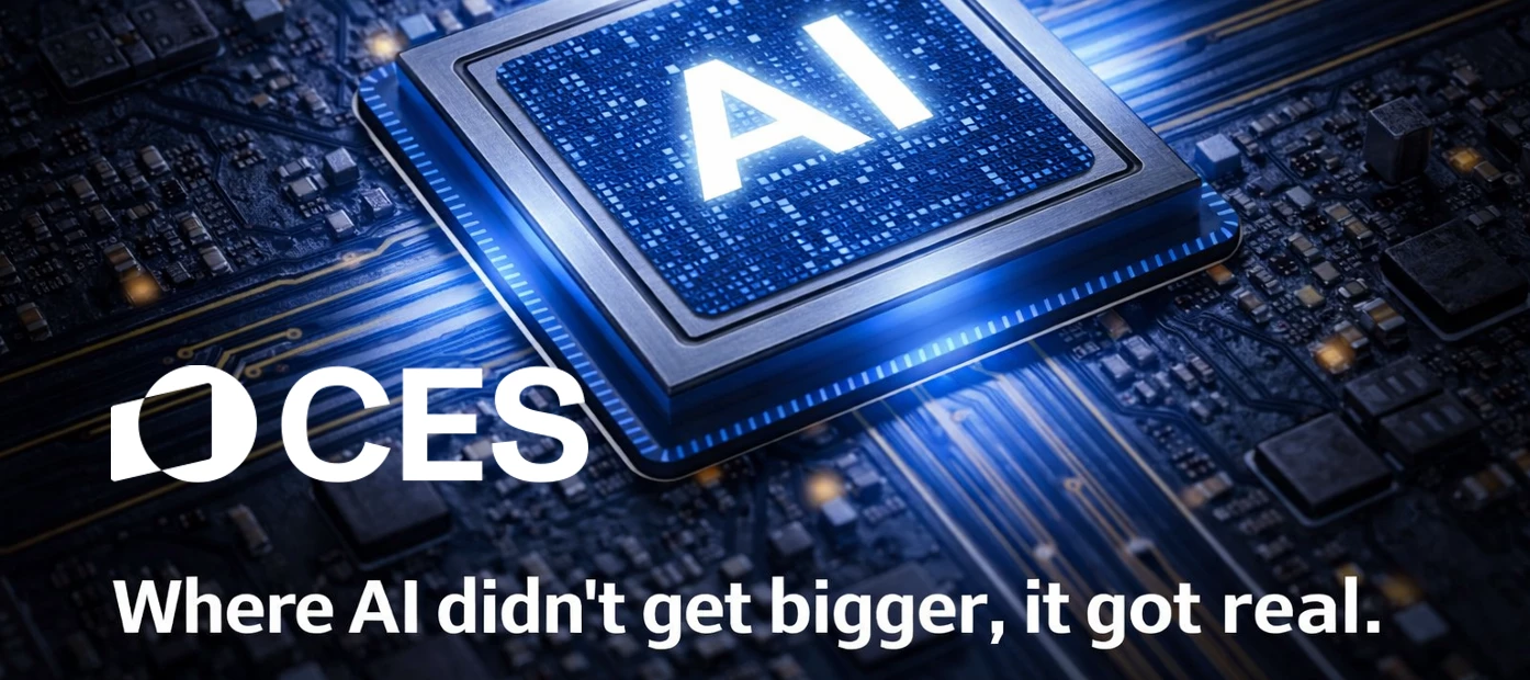
CES 2026: From AI Hype to Inference Reality at the Edge
CES has always been a bellwether for where technology wants to go. CES 2026 felt different. This year wasn’t defined by a single breakthrough announcement or the unveiling of a bigger, shinier model. Instead, it marked a quieter, but more important shift in tone.AI didn’t get bigger at CES. It got more real.Across keynotes, booths, and conversations, the focus moved away from who can train the largest model and toward a harder set of questions: How do you run AI reliably? Where does inference actually happen? And what does it take to deploy AI systems outside of a controlled demo?From Training Obsession to Inference AccountabilityThe most notable pivot at CES wasn’t a rejection of training, but instead it was an acceptance that inference is now the bottleneck.Training remains the domain of a small number of hyperscalers and frontier labs. But inference is where AI meets reality: power budgets, latency constraints, connectivity gaps, and cost ceilings. This is where architectural decisions start to matter more than peak theoretical performance.The economics tell the story. A model trained once can be deployed millions of times. Every inference event carries a cost in compute, power, and infrastructure. When you're processing video streams 24/7, analyzing sensor data in real time, or running vision models on battery-powered devices, efficiency stops being a nice-to-have. It becomes the entire business case.At CES, conversations increasingly centered on:Predictable inference cost Power efficiency and thermal envelopes Deployment complexity Offline and near-edge operationThis isn’t a shift away from training, but a decoupling of roles. Training remains the workload that creates models and capabilities. Inference underpins how those capabilities are applied, embedded, and scaled across real systems. It becomes a tool that improves and accelerates every workload, from databases and video analytics to robotics and industrial automation. In that sense, inference is no longer an afterthought. It is the defining challenge for turning AI into something usable.That’s the challenge Axelera AI was made for. At our CES suite, we demonstrated exactly what efficient inference looks like in practice: a 4-chip PCIe card capable of running up to 16 concurrent AI models processing 8K video on a single edge device. Pose detection, face recognition, and segmentation running simultaneously without thermal throttling or performance degradation.Edge AI is Here, and it’s Demanding DefinitionsAnother clear theme was the broad push by chip makers into edge AI. On the surface, this looks like diversification. Underneath, it reflects something deeper: constraints force honesty.Edge environments don’t allow for vague promises. They expose the gaps between marketing claims and deployable systems. At CES, “edge AI” was used to describe everything from embedded vision systems to rackmounted servers branded as edge appliances.That ambiguity matters because edge AI isn't just about location. It's about operating under real-world constraints that datacenter AI never faces. True edge deployments must handle thermal challenges in industrial settings, operate reliably without constant connectivity, and deliver consistent performance on limited power budgets.True edge AI raises hard questions that expose architectural choices:Can models run offline? What host system is required, and how heavy is it? How much power does inference actually consume? How easily can developers port existing models?CES made it clear that edge AI hasn’t just arrived, it’s demanding clearer definitions and greater accountability.Physical AI: Vision, Belief, and Skepticism“Physical AI” emerged as the phrase of the week, often used to describe robotics, vision-guided systems, and realtime perception. The excitement is justified. These systems represent the next wave of AI value, where software directly interacts with the physical world.Manufacturing lines that detect defects in real time. Autonomous mobile robots navigating dynamic warehouse environments. Agricultural systems that respond instantly to crop conditions. These applications unlock genuine business value by bringing AI capabilities to where physical work happens.But CES also surfaced healthy skepticism.Many physical AI demos glossed over fundamentals like deployment readiness, power consumption, or dependency on cloud connectivity. Belief in physical AI is widespread, but belief alone doesn’t ship products.For physical AI to move from concept to scale, it must be:Deterministic: producing consistent results under varying conditions Efficient: operating within strict power and thermal budgets Cloud-independent: capable of operating without constant connectivityIn short, physical AI only works when inference works. The promise of robots and intelligent systems is constrained by the same reality facing every edge AI deployment: you need reliable, efficient inference that operates in the real world, not just in controlled demonstrations.What We Heard At Axelera AI, we spent CES listening and learning, and yes, showcasing technology. The most common questions we received weren’t about peak performance, but were about practical deployment:How flexible is your SDK, and how much control do developers have over the pipeline? How difficult is it to port an existing model? What does real‑world power consumption look like? Does the system require a full host or can it work with a lightweight one? Can AI workloads run fully offline? Is the supply chain ready for production deployments?These questions signal a market that has matured. Teams aren’t experimenting anymore - they’re planning to ship.The realities of practical deployment came up with independent software vendors (ISVs) who reinforced that while promptable open-vocabulary models are generating a lot of excitement, customers are still relying on traditional closed-set models with fine-tuned datasets.We were able to work around using a vision language model (VLM) by implementing a LLM combined with a segmentation model such as the COCO dataset. There were others on the show floor implementing this same near-term solution because the point is not about cutting-edge research, but instead, production-ready engineering. While we’re excited to add VLM support this year, users can get the results they need today with this simple solution.The lesson is clear. The models that ship aren't necessarily the ones generating papers. They're the ones that work reliably, deploy easily, and deliver consistent results under real-world conditions.Building for the Inference RealityCES 2026 reinforced something we’ve believed for a long time: edge AI success isn’t defined by hype cycles or buzzwords. It’s defined by whether inference survives contact with the real world.The most compelling demonstrations at CES weren't the ones with the most impressive specifications. They were the ones solving actual business problems with measurable ROI.For example, our partner, WebOccult, demonstrated quality control for commercial bakeries, using high-frame-rate cameras and computer vision to detect, classify, and count different products moving down manufacturing lines at 90 frames per second. WebOccult was able to highly customize their solution with the Voyager SDK and complete it within 30 days. These aren't aspirational use cases. They're production systems running today, solving problems that directly impact business operations.Notable systems at CES included:Tooling that works with existing models, not against them Architectures designed for power‑constrained environments Systems that operate reliably without cloud dependencies Transparency around deployment requirementsAs edge AI moves from aspiration to reality, the industry’s focus is shifting from what could be possible to what can be deployed, scaled, and supported. The technologies that succeed won't be those with the highest theoretical performance. They'll be the ones that solve real problems under real constraints.CES didn’t mark the arrival of edge AI. It marked the moment edge AI started being taken seriously.And that’s a far more interesting place to be.
Related products:AI AcceleratorsIndustryTechnology

BlogJan 5, 2026
Axelera AI: Looking Back on 2025
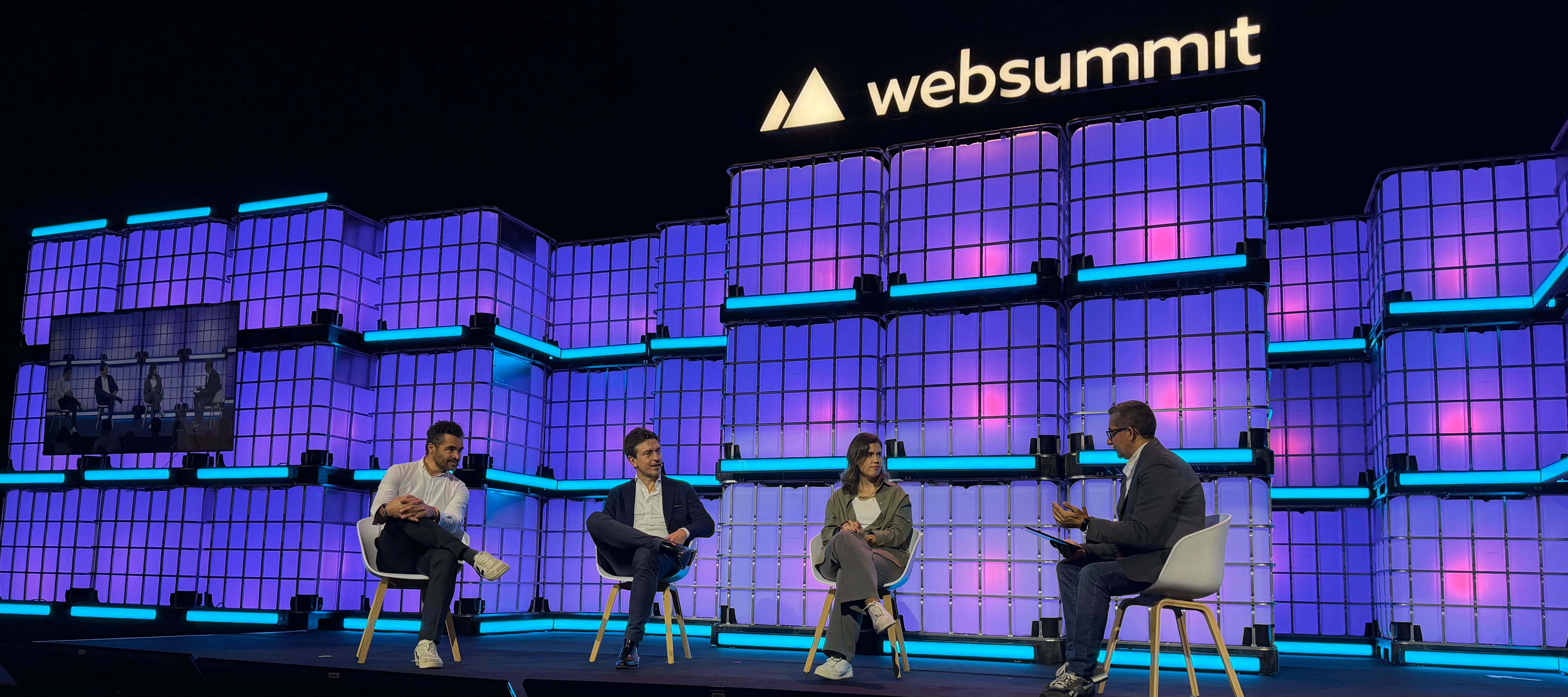
We actually anticipated a roller coaster of a year at Axelera AI in 2025, but in all honesty it’s still caught us by surprise just how much of a ride it’s been. Everything’s happened in such a whirlwind of creative techno-endeavour that it’s hard to even remember what things looked like this time last year. So it feels like the right time to reflect on what’s been accomplished, the partnerships we've built, and where we're headed next.Opening Up: Voyager SDK Goes PublicIf you can believe it, it was only back in March when we took a huge step by making the Voyager SDK publicly available on GitHub. For a company built on making AI accessible to everyone, this felt like the natural thing to do. And the response from the developer community has both proven that to be the right move, and returned a huge groundswell of support from the AI community.Since then, we've shipped four major releases: v1.2.5 (March): The public debut, packed with tools, models, and sample pipelines v1.3 (June): Added experimental LLM support, Windows compatibility, YOLO11 models, and proper thermal management v1.4 (August): Brought YOLOv10, person re-identification, and face recognition v1.5 (November): Ubuntu 24.04 support (I love this one!), Python 3.12, and our 4-chip PCIe cards Each release has increasingly been shaped by feedback from our community. Whether it's debugging customer issues or adding new models to the zoo, the collaboration has been genuinely invaluable. You have driven Voyager forward just as much as we have.Building the Developer ExperienceAlongside the SDK going public, we rolled out the infrastructure to properly support developers, partners, businesses, makers and everyone who’s as excited about AI as we are.We redesigned axelera.ai from the ground up, launched a support portal packed with guides and support docs, published a growing GitHub repo full of examples and tutorials, and opened our webstore so anyone can get their hands on Metis hardware without going through a lengthy sales process.And as you’re aware (since you’re here right now), we built this community that's now home to over 500 AI enthusiasts, members, devs and makers. Watching developers help each other troubleshoot issues, share projects, and push the boundaries of what's possible with Metis has been one of the genuine highlights of the year. There's something satisfying about seeing a Raspberry Pi user in one thread helping solve a problem for someone running a multi-stream industrial deployment in another.These touchpoints have become the foundation of how we’ll engage with AI developers from this year on. The goal was simple: make it easy to get started, easy to find answers, and easy to connect with others doing similar work. Based on the activity we're seeing, it seems to be working.Expanding Platform SupportOne of the quieter, but still vitally important stories of 2025 has been the steady expansion of platforms we officially support.The Raspberry Pi 5 is now fully supported, which was a popular request from makers and prototypers. It was actually a casual side project one of our engineers was tinkering with, but it perfomed so well it kickstarted an enthusiasm across the whole of Axelera to look much more closely at these kinds of SBC form factors. It was the springboard that saw bring-up guides for the Orange Pi 5 Plus and NanoPC-T6 quickly arriving, for those building compact, cost-effective edge deployments.For more demanding applications, we added support for Jetson Orin Nano and Jetson Orin NX, alongside systems running Intel Xeon D and W processors and AMD Ryzen 7 hosts. The Arduino Portenta X8 integration means industrial developers have a proper pathway too.The underlying philosophy here is flexibility. Whether you're a student experimenting on a Raspberry Pi, a startup prototyping on Orange Pi, or an enterprise deploying on industrial-grade x86 systems, we want Metis to just work. Each release has pushed that vision a bit further, and we can honestly say that we arrive at these milestones in exactly the same way you do - we experiement, test, iterate, fails a bunch of times, but find that the ecosystem is ultimately capable of doing whatever we can imagine.New Hardware: From Metis to EuropaOur hardware lineup grew significantly this year, with each addition shaped by what developers actually need.The 4 Quad-Core Metis PCIe card was developed to deliver a real flagship Metis device. One that packs in the inference power without taking up more space in your system. More streams, more models, more throughput. More AIPUs on one board. It's for video analytics watching dozens of cameras, or industrial systems running cascaded pipelines. If you've outgrown a single chip but don't want to rearchitect your software, this is the upgrade path we wanted to deliver.The Metis Compute Board solves a different problem. Too many customers were spending more time on host system integration than building AI applications. So we gave them a complete system: plug in power, connect a display, run inference. It's found its home in rapid prototyping, compact IoT deployments, and anywhere that "it just works" matters most. The CES Innovation Awards recognition was a nice bonus.Metis M.2 Max, announced in September, came from growing demand for LLMs at the edge. The original M.2 is brilliant for computer vision, but generative AI simply needs more memory bandwidth. M.2 Max will deliver that while keeping the same tiny footprint and low power draw, plus it's ruggedised for harsher environments.Then there's Europa, unveiled in October. This is where we're heading next: second-generation AI cores for workloads that blur the line between edge and datacenter. Multiple 4K streams, multi-user generative AI, compute density that previously meant expensive GPU infrastructure. All solved here, as the whole industry moves inevitably towards the edge.We also announced Titania, our AI inference chiplet for high-performance computing, developed as part of the EuroHPC DARE project and aimed at supercomputing applications.Europa and Titania won't ship until 2026 and beyond, but 2025 was the year they came to life. Even as we shipped Metis products to customers, our hardware teams already had an eye on what needs to come next.Funding and SupportIn March, we secured €60 million in funding from the EuroHPC Joint Undertaking and member states. This wasn't just money though; it was validation that Europe is serious about building sovereign AI infrastructure. Combined with our previous Series B funding, we've now raised over $200 million. That’s a lot of faith that the sector and the region have placed in Axelera AI.We were also selected for the EIC Step Up programme, which provides significant additional equity investment to help scale operations. As Bloomberg reported in August, we're deep in discussions for an additional round to expand our edge AI and datacenter activities even further next year.Building an EcosystemOne of the highlights of 2025 was formalising partnerships that genuinely matter. Not just to us, but to the European AI sector in general.Our collaboration with Arduino, announced late last year, came to life at CES in January. Pairing our Metis accelerators with Arduino's Portenta modules means millions of developers can now access proper AI acceleration in a familiar environment. It's exactly the kind of democratisation we set out to achieve from day one.In June, we launched the Partner Accelerator Network with founding members including Aetina, Arduino, Astute, C&T Solution, Eurocomposant, Macnica, and Seco. This isn't just a logo wall to fancy up our website, by the way. It's a actual, active ecosystem of partners helping customers move from proof-of-concept to production. It’s the bedrock of what Axelera’s building.The partnership with the European Space Agency deserves a special mention, too. ESA chose Axelera because of our sovereign technology and long-term availability. When your hardware might spend a decade in space, those things matter. It's humbling to think our chips could help answer some of the universe's biggest questions (and it’s just cool as hell to have your gear in orbit!).We've also deepened ties with Lenovo, Dell, Advantech, and Micron, and validated our platform on BalenaOS for fleet deployments. And most recently, we teamed up with YOLO model creator Ultralytics, in what’s set to be an epic leap forward now our cutting-edge acceleration is seamlessly integrated into the Ultralytics models. You can see more about that in the video below.Showing UpWe've been crazy busy at industry events this year too. Highlights include: CES 2025 in Las Vegas, where we were named a CES Innovation Awards Honoree for the Metis Compute Board Embedded World 2025 in Nuremberg, showcasing solutions with duagon and Arduino ISC West 2025, where we demonstrated real-time YOLOv8l inference on 8K video COMPUTEX 2025 in Taiwan, displaying our growing partner ecosystem Web Summit 2025 in Lisbon, discussing sovereign AI We've also participated in important European policy discussions, including the AI Continent Action Plan launch in Brussels, the French AI Action Summit, and the State of Dutch Tech.What It All MeansLooking at 2025 in totality, a few themes emerge.First, edge AI is real and 2025 is the year it arrived for everyone. The gap between what's theoretically possible and what actually works in production environments is rapidly closing. Our customers are deploying real solutions for retail, manufacturing, security, transportation and more.Second, European tech sovereignty matters. The funding, the partnerships, the policy engagement. There's a genuine momentum behind building AI infrastructure that isn't dependent on a single geography or vendor.Third, and most importantly, none of this happens without the community. The developers filing issues on GitHub, the partners building solutions, the customers pushing us to do better. Thank you all for joining us.What's NextEuropa ships in 2026. The M.2 Max won’t be far behind. Titania is well on track, too. We'll keep improving Voyager SDK based on what you tell us you need. And we'll keep working to make AI accessible, efficient, and genuinely useful.As our CEO Fabrizio likes to say: it's still day one. The best is yet to come.
Related products:Company
BlogNov 12, 2025
The Hidden Third Dimension of Edge AI: Why Infrastructure Origin Matters
Most companies evaluate edge AI hardware on two dimensions: performance and cost. A third dimension has been a hot topic at tech events from Taiwan to Portugal: sovereign AI.Infrastructure origin matters. Here's why.Three Business RisksRisk 1: Supply ContinuityRemember when Russia was cut off from SWIFT? When Huawei lost access to U.S. chips? When pandemic disruptions exposed supply chain vulnerabilities?Foreign-controlled AI infrastructure faces the same risks. During geopolitical tensions, access can be restricted, sabotaged, or simply repriced. Companies dependent on that infrastructure have no alternatives.Real scenario: You've deployed edge AI across 5,000 retail locations. Your hardware vendor's supply chain gets caught in trade restrictions. You can't get replacement units, can't expand to new locations, can't maintain existing deployments.This isn't theoretical. It's happened repeatedly with other critical technologies.Risk 2: Data Sovereignty and Regulatory ComplianceRegulatory requirements increasingly mandate where data can be processed and stored. GDPR was just the beginning. Industry-specific regulations for healthcare, finance, and critical infrastructure now specify data residency requirements.The problem: If your edge AI solution processes locally but the hardware, firmware, or model updates route through foreign-controlled infrastructure, you may not actually be compliant.Real scenario: Your industrial AI application processes employee biometrics or proprietary production data. Regulations require local processing. But your hardware vendor's telemetry, updates, or support infrastructure crosses borders you can't control.The compliance risk isn't obvious until an audit exposes it.Risk 3: Competitive PositioningAI productivity gains flow to wherever the infrastructure is controlled. When you depend on foreign platforms, you're optimizing for their ecosystem, their models, their roadmap.Real scenario: You build vertical-specific AI capabilities on a closed platform. Your solution works well, but you can't differentiate because you're constrained by what the platform supports. A competitor using open architecture can optimize for your specific market requirements.Generic global AI can't match locally optimized solutions for specific industry needs.What Sovereign AI Actually Means (Practically)True sovereignty means independent capability across the full technology stack: chip design, manufacturing, compute infrastructure, models, data pipelines, and deployment environments.Reality check: Complete independence is unrealistic and economically unjustifiable for most organizations and even many nations. Building semiconductor fabs requires enormous investment.Viable path: Regional sovereignty through open architectures and strategic collaboration.This is why open standards like RISC-V matter. You're not locked into a single vendor's proprietary ecosystem. You maintain strategic control while benefiting from ecosystem collaboration.Europe, the United States, and allied nations can pool resources and ensure equal access to AI infrastructure that doesn't create dependency on adversarial powers.See what Fabrizio’s take was from the discussion at Websummit in Lisbon 2025:The Axelera AI ApproachAxelera builds on RISC-V instruction set architecture with European innovation and manufacturing relationships. This isn't just technical preference. It's strategic capability.What this means for customers:No vendor lock-in: Open architecture means you can optimize for your specific requirements without being constrained by proprietary limitations.Supply chain resilience: Regional manufacturing and partnerships reduce exposure to single-geography disruption.Compliance clarity: European data protection standards built in from architecture level, not retrofitted.Competitive differentiation: Purpose-built solutions for your industry rather than generic platforms adapted from consumer applications.As Fabrizio Del Maffeo put it at a recent talk at AI Beyond The Edge forum: "Our mission is ensuring that businesses and nations have the AI infrastructure they need to innovate without compromise, defend without dependence, and lead without limits."Evaluating Your Current Edge AI StrategyThree questions most companies don't ask until they face problems:If geopolitical tensions escalate, can you still get hardware, firmware updates, and support? Map your vendor's supply chain and support infrastructure. Does your edge AI solution actually meet data sovereignty requirements, or are there hidden dependencies on foreign-controlled infrastructure for updates, telemetry, or model management? Can you optimize your AI implementation for your specific market, or are you constrained by a closed platform's roadmap and priorities?Smart operators are evaluating these dimensions now, before crisis forces reactive decisions.The Organizations Moving FirstCompanies that already faced supply chain disruptions or regulatory compliance challenges understand this viscerally. They're evaluating edge AI vendors not just on spec sheets but on:Architecture openness (RISC-V vs. proprietary) Regional manufacturing capabilities Data sovereignty by design Ecosystem collaboration without lock-inThe race for deployable, strategically sound edge AI is already underway. The organizations moving now recognized that where your infrastructure comes from matters as much as what it can do.Evaluate infrastructure strategy:Explore open architecture approach: store.axelera.ai Join strategic discussion: community.axelera.ai
Related products:AI Accelerators
Oct 30, 2025
Why Edge AI Deployments Are Stalling (And What's Finally Changing)
The paradox: Enterprise AI adoption stands at 44.5% across U.S. businesses. The edge AI market is growing at 21.7% CAGR. Yet most companies remain stuck in pilot purgatory, unable to scale beyond proof-of-concept.At last week's AI Beyond The Edge forum, Axelera AI CEO Fabrizio Del Maffeo addressed this head-on: "There's a massive disconnect between what everyone's talking about and what's actually working in the real world."Here's what's really holding companies back.The Infrastructure Doesn't Match the RequirementsThe market is ready. AI compute costs have dropped from thousands to hundreds of dollars. Models are proven. But when companies try to deploy at scale, they hit the same walls:Retail operators report that other edge setups can't handle the latest computer vision models. Hardware overheats in store environments or proves too costly to scale across thousands of locations.Industrial customers face a painful choice: solutions that consume too much power (adding $500+ to monthly electricity bills per deployment) or hardware that thermally throttles under factory conditions.Smart city planners calculate ROI and walk away. Processing 4K/8K video streams for traffic optimization and public safety has been prohibitively expensive with GPU solutions.Agricultural and medical applications need 24/7 operation in challenging environments without breaking the budget on power costs. Most hardware can't deliver both reliability and efficiency.The pattern is consistent across industries: what works in controlled lab environments fails in production.Fabrizio Del Maffeo, CEO of Axelera AI, speaking at AI Beyond The EdgeWhy Adapted Solutions Can't Solve Edge ProblemsDel Maffeo's diagnosis: "Everyone's trying to shove cloud chips or mobile processors into edge applications. The underlying architecture just wasn't built for this job."The technical reality: neural networks spend 70-90% of their time on matrix-vector multiplications, whether processing speech recognition, natural language, or computer vision. Traditional computer architectures constantly move data back and forth between memory and processing units.For edge applications where every milliwatt matters, this approach wastes energy. You're spending most of your power budget on data movement rather than actual computation.The result: Hardware that looks impressive on spec sheets but can't maintain performance in real-world conditions, at real-world power budgets, at prices that make deployment viable across hundreds or thousands of endpoints.What Changes When Architecture Matches WorkloadAxelera AI’s purpose-built edge AI architecture places memory and compute elements directly adjacent, dramatically reducing data movement. This isn't about being faster at everything. It's about being optimal for the operations that define modern AI workloads.When architecture matches requirements, applications that were theoretically possible become economically practical:Kitchen Monitoring (Food Service)The challenge: Verify cook uniform compliance for up to 20 people per camera in real-time without adding staff.What's now possible: Simultaneous processing at 45 FPS for person detection plus 900 FPS for uniform verification on a single edge device.Business impact: Food safety compliance automation that actually works in commercial kitchen conditions.Seed Sorting (Agriculture)The challenge: Complete the entire cycle in 4ms total (image capture + AI processing + actuation decision).Previous solutions: High-end GPUs like Nvidia RTX 4080 required 2.3ms for AI processing alone, failing to meet the requirement.What purpose-built enables: 1.2ms AI processing, making the use case viable with margin for image capture and mechanical actuation.Business impact: Throughput that justifies the equipment investment.Manufacturing Quality ControlThe challenge: Run multiple inspection models simultaneously across production lines without excessive power draw or thermal throttling.What's now possible: Consistent performance in actual factory environments, processing multiple camera feeds in parallel.Business impact: 30% reduction in quality issues with 50% lower inspection costs compared to manual processes.High-Resolution Smart City ApplicationsThe challenge: Process 4K/8K video streams from multiple cameras for people detection, tracking, and traffic analysis.What's now possible: Multi-core architecture and a robust SDK that handles high-definition streams without requiring prohibitive infrastructure investment.Business impact: ROI that makes municipal deployment viable rather than aspirational.What This Means for Your Evaluation ProcessIf your edge AI pilot didn't scale, the problem likely wasn't your use case or your team's capabilities. It was probably the hardware.Three questions to reconsider:Were your ROI calculations based on hardware built for cloud or mobile, then adapted for edge? If so, your performance and power assumptions may have been optimistic by 3-5x. Did your pilot succeed in the lab but fail in production conditions? Thermal performance under sustained load in real environments often differs dramatically from spec sheets. Was the per-unit cost acceptable for 10 devices but prohibitive for 1,000? Hardware that wasn't designed for edge economics from the ground up rarely scales to production volume pricing.The gap between AI potential and AI deployment is closing, but only for organizations evaluating purpose-built infrastructure rather than adapted solutions.Next week: Why performance and cost aren't the only considerations. The strategic dimension most companies are missing when evaluating edge AI infrastructure.Evaluate your edge AI strategy:Technical resources: github.com/axelera-ai-hub/voyager-sdk Community discussion: community.axelera.ai
Related products:AI SoftwareAI Accelerators

BlogOct 21, 2025
Breaking the Edge Performance Ceiling
New AIPU, Europa, Delivers Datacenter-Class AI Performance in Server Form Factors Without the Datacenter Price Tag by Manuel Botija, VP of Product Management Axelera® AI announces Europa®, our next-generation AI Processing Unit (AIPU) launching in the first half of 2026, purpose-built to let businesses right-size their AI deployments for demanding edge or enterprise datacenter workloads.Europa creates a new class of AI acceleration to complement the lower-powered sibling, Metis®, extending our product portfolio to serve more demanding workloads while maintaining the outstanding power efficiency Axelera is known for. At just 45 watts, Europa delivers 3 to 5 times better performance per watt and performance per dollar efficiency than GPUs, making datacenter-class AI performance accessible for edge and enterprise server deployments.The result? Businesses no longer need to compromise between performance and cost when deploying AI at the edge.Why AI Needs Multiple Performance Tiers, Especially at the EdgeThe future of AI extends far beyond the datacenter. While cloud solutions are driving widespread AI adoption, transformative innovation is also happening at the edge. Businesses are applying intelligence to existing infrastructure in ways that fundamentally change operations:Security cameras that understand threats, not just detect movement Manufacturing defect inspection on production lines Retail systems that personalize experiences in real-time, right at the point of interactionAcross industries, organizations are discovering countless opportunities to optimize their businesses with on-device AI processing. These applications can work independently or integrate seamlessly with cloud infrastructure, but the local intelligence is what unlocks capabilities and responsiveness that weren't possible before.Here's the thing: many of these applications need local processing power. They can't wait for round trips to the cloud when split-second decisions matter. But edge deployments aren't one-size-fits-all. A single-camera quality control system has completely different requirements than a multi-user generative AI application processing dozens of video streams at once.That's where many businesses hit a performance ceiling. Ultra-low-power edge chips work beautifully for simpler workloads. But when you need to run multi-modal AI, support multiple concurrent streams and users, or process complex AI models locally, suddenly you're looking at a gap between what edge devices can handle and what expensive datacenter solutions provide.Until now, the answer has been GPU solutions designed for datacenters. But those come with costs, power requirements, and infrastructure demands that make edge deployment impractical.That's the gap we designed Europa to address. It's built to handle AI workloads that are too demanding for sub-10-watt edge solutions, but don't need the expense and complexity of datacenter GPUs. Better performance where you need it, without the infrastructure overhead you don't.Europa Enables Advanced AI Applications at the EdgeEuropa is purpose-built for the demanding workloads that exist at the edge, on-device rather than in the cloud. By delivering 629 TOPS in a 45-watt, standard PCIe form factor, Europa makes demanding applications practical and affordable.Europa is built for the applications that need higher performance per chip:Manufacturing and industrial automation processing multiple camera streams simultaneously for quality control, or combining computer vision with generative AI for complex defect analysis.Smart infrastructure and security running intelligent surveillance with on-prem multi-user capabilities, or managing traffic systems that need real-time vision and prediction models.Automotive infotainment and robotics requiring multi-camera fusion, robots with integrated vision-language processing, or fleet systems with on-vehicle generative AI.Enterprise servers and workstations supporting multi-user generative AI applications, development platforms for AI sovereignty initiatives, or accessible enterprise-grade infrastructure for research and mid-market companies.With a single Europa chip, you get performance that would require multiple Metis chips to achieve. With integrated pre- and post-processing and a built-in hardware decoder, Europa enables high-performance AI at the edge without the need for costly CPUs, thereby lowering the solution’s total cost of ownership (TCO).Europa builds on Metis's proven efficiency to unlock new performance territory. Delivering 5 times better performance in computer vision and up to 70 times improvement in multi-user generative AI applications, Europa creates a new tier of edge AI capabilities. This leap in performance opens entirely new categories of applications that were previously confined to datacenter deployments.Technical Innovation Enabling Real World ValueEuropa's performance advantage comes from precision-engineered innovations designed specifically for edge deployment constraints.Integrated intelligence reduces system complexity:Second Generation AI Cores featuring Digital In-Memory Compute (D-IMC) deliver exceptional efficiency by supporting any AI modality such as vision, audio, or language, and a wide range of AI architectures, including CNNs, ViTs, and LLMs 16 RISC-V vector cores handle pre- and post-processing and an integrated H264/H.265 hardware decoder processes 4K video at 120FPS on-chip, freeing your host CPU for business logic Enhanced memory architecture with 128MB L2 SRAM and 200GB/s bandwidth solves the memory bottleneckDesigned for flexible deployment:Single-chip PCIe card configurations starting with 16GB for edge server applications Four-chip PCIe card systems with up to 256GB for enterprise deployments requiring maximum throughput Same software architecture using the Voyager SDK across all configurations for develop-once, deploy-anywhere simplicityOpen platform accelerates development:Voyager SDK available on GitHub empowers developers with transparent tools and resources Minimal code changes required when scaling from Metis to Europa platforms Europa will be available on the Axelera AI web store and from channel partners for easy acquisitionChoosing the Right AI Performance Tier Axelera AI now offers performance tiers to match your specific edge AI requirements. Our platform approach means you can start with the right solution today and scale seamlessly as your needs evolve, all while using the same development tools and software stack. Application Requirements Metis AIPU Europa AIPU Best Suited For Embedded and industrial systems, ultra-low-power edge AI Professional workstations, edge servers, enterprise deployments, multi-user applications Peak Performance 214 TOPS 629 TOPS Average Power 4 to 8 watts 20 to 45 watts Available Form Factors M.2, PCIe cards, compute boards PCIe cards in 1-chip and 4-chip configurations Ideal Use Cases 1-16 camera computer vision, on-device small language models, power and thermal constrained devices 16-64 camera systems, generative AI applications, multi-modal workloads, server deployments Language Model Capability Up to 8B parameters per chip Up to 32B parameters per chip, 70B+ parameters across multi-chip systems The guiding principle is straightforward: Start with Metis for ultra-efficient edge deployments where power constraints are critical. Scale to Europa when your application demands server-class performance but you need to maintain edge deployment economics and form factors.Both products share the same underlying architecture and development tools, so your investment in learning one platform transfers directly to the other.Making Advanced AI Accessible for More BusinessesEuropa embodies Axelera AI's founding mission: advanced AI capabilities for everyone building the future. By delivering 3 to 5 times better performance efficiency than traditional solutions, Europa makes applications economically viable that were previously reserved for organizations with datacenter budgets.Key advantages:Performance per dollar ratio opens new application categories for mid-market companies and innovative startups Standard form factors mean existing IT teams can deploy and manage Europa without specialized training Power efficiency enables deployment where datacenter-class power infrastructure is not available or practical European innovation designed for global implementationThe combination of accessible pricing, familiar integration methods, and outstanding efficiency means businesses of all sizes can now deploy the AI capabilities they need to compete and innovate. When advanced AI hardware is affordable and efficient, novel solutions become possible that transform industries.Learn More About Europa AI Processing UnitReady to deploy datacenter-class AI performance at the edge?Europa begins shipping in the first half of 2026 with PCIe card configurations designed for seamless integration into your existing infrastructure. In the meantime, you can sign up for upcoming product briefs and further details or apply for the limited early access program.Axelera AI is making advanced AI capabilities accessible to everyone building the future. Europa represents the next step in that mission, bringing powerful, efficient, and affordable AI acceleration to the deployments that will transform industries.
Related products:AI Accelerators
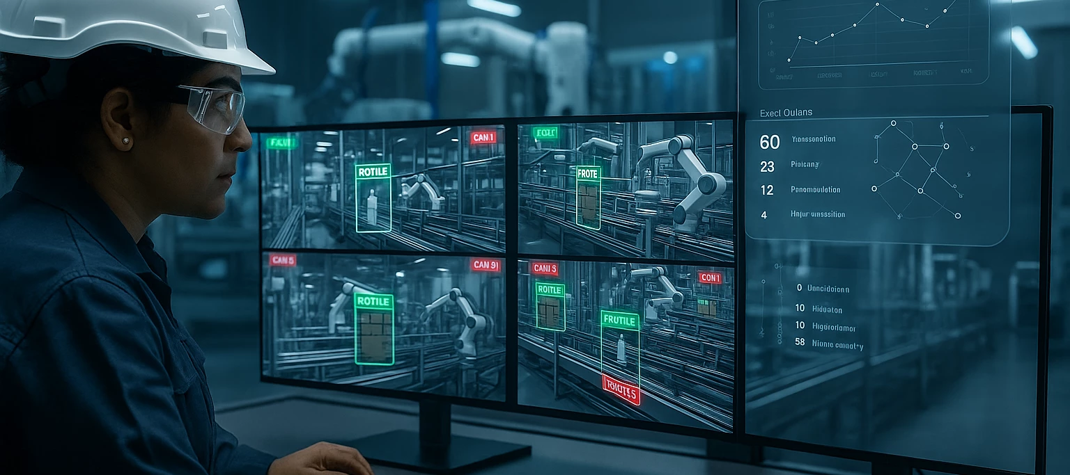
BlogAug 20, 2025
A New Edge AI Hardware Option for BalenaOS
Developers and engineers looking for new options for their fleets of devices using edge AI are getting them.BalenaOS has become popular precisely because it solves real deployment problems. The container-focused operating system enables over-the-air updates, remote management, and scalable fleets across embedded and edge devices.This approach works perfectly for large-scale solutions in smart retail, healthcare, autonomous systems, robotics, and manufacturing. The challenge has been finding AI hardware that matches balenaOS's deployment philosophy.Current solutions often create vendor lock-in and setup complexity that defeats the purpose of choosing balenaOS in the first place. New AI accelerators solve this problem by delivering right-sized performance that integrates naturally with container-native workflows. Businesses can optimize both system performance and power consumption without sacrificing the deployment flexibility that makes balenaOS valuable.Axelera® AI's Metis® AIPU is purpose-built for computer vision and LLM inferencing at the edge with the best performance-to-cost ratio in the market. Metis' ease of use is the perfect match for balenaOS, so we set out to test whether we could bring this powerful combination to innovators at the edge.What We TestedOur validation was performed on an x86-based Lenovo P360 Ultra workstation, equipped with a Metis PCIe card. We used Voyager SDK version 1.3.3 and built a custom balenaOS image tailored for this setup. The goal was to enable full inference capabilities within a Docker container running on balenaOS, using the Metis accelerator.Out-of-the-box balenaOS images do not include certain kernel features required by the Metis driver; specifically, support for system DMA-BUF heaps. Without these, the driver cannot access the necessary memory interfaces, preventing inference workloads from executing.To address this, we built a custom balenaOS image from source, enabling the required kernel options. This involved identifying the correct device configuration for our x86 platform, modifying kernel build parameters, and compiling the OS using balena’s Yocto-based build system.Driver and SDK IntegrationOnce the custom OS was in place, we compiled the Metis driver against the specific kernel version used in our balenaOS build. This step is critical, as balenaOS does not support DKMS, so drivers must be built manually for each kernel variant.With the driver installed and loaded, we deployed the Voyager SDK inside a Docker container. Using a prebuilt image that includes all necessary runtime components, we configured the container to access the Metis device and other system resources required for inference.Running Inference on balenaOSAfter setting up the environment, we successfully ran inference workloads using the Voyager SDK inside the container. The system was able to process video input and deliver high-throughput inference performance, confirming that the Metis accelerator is fully functional under balenaOS.To streamline future deployments, we also created a startup script that prepares the device environment on boot, loading the driver, setting permissions, and configuring device links so that inference can begin immediately after power-on. Why This MattersThe combination of Metis processing power and balenaOS flexibility creates new possibilities for production-scale edge AI in practical deployment scenarios.Retail AI at the Edge Multi-camera video analytics becomes feasible at scale. Think queue tracking across multiple checkout lanes, shelf monitoring for inventory management, or customer behavior analysis across store sections. Metis handles the stream concurrency that these applications demand, while balenaOS manages secure fleet updates across hundreds of retail locations without requiring on-site technical staff. Intelligent Transport Monitoring Vehicle-mounted systems can now run sophisticated AI workloads locally. License plate recognition, passenger analytics, and incident detection operate on low-power hardware, like Metis’ 8-15 watts, with real-time processing capabilities. When new models or detection algorithms become available, balenaOS delivers over-the-air updates to entire transit fleets without service interruption. Factory Floor and Infrastructure Inspection High-resolution defect detection systems can deploy across manufacturing environments with enterprise-grade management. Metis hardware even supports LLM-based analysis for complex inspection scenarios. Container-based deployment provides the audit trails and version control that regulatory environments require, while Metis delivers the processing power needed for real-time quality control.The low cost and ease of deployment mean development teams can test and iterate new systems and solutions with speed and flexibility.Looking AheadThis validation advances our core mission: ensuring that breakthrough AI capabilities are within reach for every innovator building edge applications. If you’re working on an edge AI project and see potential in this approach, feel free to ask any questions on implementation below, share ideas for adapting it to your use case, or just tell us about the project you're building so we can help you get there.
Related products:AI SoftwareAI AcceleratorsTechnology

BlogJun 30, 2025
Why Edge AI Is the Next Frontier and Why Today's Solutions Aren't Good Enough
I've been thinking a lot lately about where we are with AI. Not the hype, not the headlines, but the reality of what's actually happening on the ground with real customers trying to solve real problems.And honestly? There's a massive disconnect between what everyone's talking about and what's actually working in the real world.Let me explain what I mean.We're heading toward AI everywhere whether we're ready or notLook, the trajectory is pretty clear if you step back and look at the big picture. We went from approximately 10 million mainframes back in the 60s-80s to 2 billion PCs by 2005. Now we've got over 50 billion connected devices, and we're racing toward 100+ billion devices that demand some form of intelligence built in.This isn't just tech evolution, it's economics. Three things are driving this shift that nobody can ignore:AI compute costs are dropping fast – what used to cost thousands now costs hundreds Cloud AI hits a wall when you need real-time responses for billions of devices The value you get from AI goes through the roof when it's right where you need itThink about it this way: if you're running a retail store, you can't have your self-checkout system waiting for a round trip to some data center in Virginia every time someone scans a banana. An industrial robot can't pause for 200 milliseconds to "think" about whether to grab that part or not, or worse, to stop if a worker crosses its path. A smart traffic system can't afford to have every camera upload video to the cloud just to figure out if the light should change. A car can’t wait for the network to decide whether to turn right, left, or correctly recognize a danger.The math does not work. The problem: current solutions are... not greatHere's what really gets me. Despite this obvious need, the solutions out there are just not cutting it. I see this every single day when I talk to customers across different industries, and across regions.Retail experts tell me their current edge AI setups can't handle the latest computer vision models they need. The hardware isn't fast enough, it overheats in their environment, or it is too costly to scale across thousands of stores or point-of-sale systems.Industrial customers say everything available is either too power-hungry (try explaining a $500/month electricity bill increase to procurement) or gets thermally constrained the moment you put it in a real factory setting.Smart city deployments? Most cities take one look at the price tag and just walk away. The ROI isn't there with current solutions.Medical and agritech applications need something that can run 24/7 without breaking the bank on power costs, and frankly, most of what's available today just can't deliver.The fundamental issue is that everyone's trying to shove cloud chips or mobile processors into edge applications. It's like trying to use a freight train for Formula 1 racing – the underlying architecture just wasn't built for this job. Why the cloud-first approach is hitting its limitsTruly disruptive technologies often begin in a centralized form, requiring significant investment and intensive experimentation. As the technology matures, it gradually decentralizes.Take electricity: we started with massive, centralized power plants, but today we’re moving toward distributed systems—solar panels on rooftops and, potentially in the future, compact nuclear reactors powering individual homes or neighborhoods.The same trend applies to computing. Centralized mainframes evolved to personal computers, and now to smartphones in every pocket.We’re seeing the same pattern unfold in quantum computing, and it’s already happening with AI. The evolution in computing, software and neural network architecture are making edge AI (physical AI) come true.Meanwhile, latency, privacy concerns, or regulatory requirements for keeping data local are accelerating the expansion of AI from cloud to edge devices. The math that matters: it's all about matrix operationsRunning real artificial intelligence in a constrained environment like inside edge devices requires a completely new hardware and software architecture.Let me get a bit technical for a minute, because this is where it gets interesting.Neural networks are basically doing matrix-vector multiplications (MVMs) about 70-90% of the time, whether you're doing speech recognition, natural language processing, or computer vision. That's just the reality of how these models work.Traditional computer architectures are constantly moving data back and forth between memory and processing units. For edge applications where every milliwatt matters, this approach is just wasteful. You're spending most of your energy budget on data movement rather than actual computation.The solution? You need to rethink the silicon architecture completely. Put memory and application specific compute elements right next to each other, reduce data movement, shrink the physical footprint, and dramatically increase throughput for these MVM operations.This is where digital in-memory computing architectures really shine. They're built specifically for the mathematical operations that define modern AI workloads. It's not about being faster at everything; it's about being optimal for the things that actually matter. The real challenge is making high performance accessibleBut solving the hardware problem is only half the battle. The real breakthrough happens when you make this performance accessible to developers and innovators who aren't chip designers.This means comprehensive software development kits that hide the complexity while delivering the full performance benefits. It means modular solutions: M.2 cards, complete edge servers, whatever fits into existing infrastructure without requiring a complete overhaul.And most importantly, it means pricing that makes sense for real-world deployments, not just proof-of-concept demos. The sectors that are ready to explodeThe opportunity is huge because so many industries are basically waiting for solutions that actually work:Retail and hospitality need computer vision that's reliable and fast enough for real-time applications, but current solutions are either too expensive or too unreliable for widespread rollout.Energy and utilities want distributed intelligence for grid management and predictive maintenance, but existing edge AI hardware can't handle the environmental requirements and uptime expectations.Manufacturing and robotics need real-time decision-making that current solutions simply can't deliver at the right price points and power budgets.Smart cities might be the biggest opportunity of all: traffic optimization, public safety, infrastructure monitoring. They all require local processing that doesn't exist at scale today.These aren't niche applications. These are massive markets waiting for technology that actually works. What comes nextThe companies that will win the next wave of AI deployment in the physical world won't be the ones with the biggest cloud infrastructure or the most general-purpose chips. They'll be the ones who figured out early that edge AI needs purpose-built solutions: hardware and software designed from scratch for distributed intelligence.This isn't some future scenario. It's happening right now. The question isn't whether we'll see ubiquitous AI deployment. We will. The question is which architectures and which companies will make it possible most effectively.As we build toward this future, I think there are three things that really matter: delivering genuine performance improvements over what exists today, making that performance accessible through intuitive tools, and pricing it for mass adoption rather than just high-end applications.The next frontier of AI isn't in the cloud, it's everywhere else, around us. (Should we say in the physical world?) And honestly, I think the companies that get this first are going to define the next era of computing.It's still day one, and the best is yet to come.
Related products:Industry
BlogJun 17, 2025
Voyager SDK: Release Update with New Features
At Axelera AI, we’re committed to advancing edge AI with every release, and Voyager SDK v1.3 is no exception. This quarterly update brings meaningful improvements that expand platform compatibility, introduce support for new models and use cases, and enhance system control and usability.Along with the new features, we have continued optimizing the execution of neural networks on our Digital In-Memory Computing engine to deliver higher performance and efficiency. Users will see measurable gains across major model families, another step forward in delivering a reliable, production-ready platform for AI innovation.We are also including experimental features to get feedback and share our innovations with you all - including the Tiled inference seen below in the video. Using YOLOv11, we are detecting people at high-resolution (4K). By leveraging our native tiled inference feature, developers can get an order-of-magnitude improvement in detections vs. the conventional approach of inferencing against a downscaled input video. You can find Voyager SDK v1.3 on GitHub now. New Features of v1.3The latest version of Voyager SDK introduces enhancements that cater to advanced AI use cases while broadening platform support. Among the standout features are:Support for Large Language Models (LLMs): The SDK now supports LLMs and offers LLM-based applications, such as chatbots, seamlessly. You may have seen one of our engineers showcasing this lately at major industry events, or online here. Native Support for Microsoft Windows: Both Windows 10/11 and Microsoft Windows Server 2025 are now supported on x86-based systems, making deployment easier and more versatile. Hybrid CNNs with Attention Layers: In alignment with cutting-edge AI research, the SDK supports hybrid convolutional neural networks (CNNs) incorporating attention layers, including models like YOLO11. Computer vision applications using these models can benefit from state-of-the-art accuracy on a large number of concurrent real-time video streams. Thermal Management Features: Thermal management enables a wider operating temperature range for our hardware and includes thermal protection and thermal control features. Expanded Host Support: Out-of-the-box compatibility now includes AMD Ryzen 7 and NXP iMX8-based hosts, enabling performance optimization across diverse setups. Dynamic Fan Control: We heard you – the fan was loud when running at full speed. We have now added a control that reduces the speed of the fan when the cards are not operating at high temperatures. Observability: a system service and Graphical User Interface (GUI) for monitoring Metis devices increases visibility in the utilization of our hardware. Model Additions and Enhancements: Model ZooVoyager SDK’s Model Zoo continues to grow. Below is a list of all the models we support now, having added 30 new models and formats natively within the SDK. Beyond our Model Zoo, we have verified additional models (also below) from HuggingFace’s TIMM model collection; to deploy any of these, you can use the existing ax_models/zoo/timm/mobilenetv4_small-imagenet.yaml as a template and update the timm_model_args.name field to your desired model and adjust the preprocessing configuration as needed. Performance GainsOur team was primarily focused on ensuring missing features and functionality were delivered in this release. However, even while focusing on net-new advancements, you will find performance boosts across all of the model families. The chart below shows average gain from our prior release to this one. These speed increases represent work we are doing with customers as well, which we are delivering to the entire community when the changes are widely applicable. average performance gains in Voyager SDK v1.3 per network family What’s Next? While this release includes exciting advancements, our journey is far from over. We remain committed to a quarterly release cycle and listening to feedback from our community. If you have not yet joined, please join the Axelera AI Community and help contribute to the upcoming roadmap! Image Classification (18 models) Model Name Resolution Format Squeezenet 1.0 224x224 PyTorch, ONNX Squeezenet 1.1 224x224 PyTorch, ONNX Resnet-18 224x224 PyTorch, ONNX Resnet-34 224x224 PyTorch, ONNX Resnet-50 224x224 PyTorch, ONNX Resnet-101 224x224 PyTorch, ONNX Resnet-152 224x224 PyTorch, ONNX Resnet-10T 224x224 PyTorch, ONNX MobilenetV2 300x300 PyTorch, ONNX MobilenetV4-small 224x224 PyTorch, ONNX MobilenetV4-medium 224x224 PyTorch, ONNX MobilenetV4-large 384x384 PyTorch, ONNX MobilenetV4-large (w/ AvgPool Anti-Aliasing) 384x384 PyTorch, ONNX EfficientNet-B0 224x224 PyTorch, ONNX EfficientNet-B1 224x224 PyTorch, ONNX EfficientNet-B2 224x224 PyTorch, ONNX EfficientNet-B3 224x224 PyTorch, ONNX EfficientNet-B4 224x224 PyTorch, ONNX Object Detection (26 models- Blue are new) Model Name Resolution Format SSD-MobileNetV1 300x300 ONNX SSD-MobileNetV2 300x300 ONNX Yolov3 640x640 ONNX Yolov5n-v7 640x640 PyTorch, ONNX Yolov5s-relu 640x640 PyTorch, ONNX Yolov5s-v5 640x640 PyTorch, ONNX Yolov5s-v7 640x640 PyTorch, ONNX Yolov5m-v7 640x640 PyTorch, ONNX Yolov5l-v7 640x640 PyTorch, ONNX Yolov7 640x640, 640x480 PyTorch, ONNX Yolov7-tiny 640x640 PyTorch, ONNX Yolov8n 640x640 PyTorch, ONNX Yolov8s 640x640 PyTorch, ONNX Yolov8m 640x640 PyTorch, ONNX Yolov8l 640x640 PyTorch, ONNX Yolov9t 640x640 ONNX Yolov9s 640x640 ONNX Yolov9m 640x640 ONNX Yolov9c 640x640 ONNX Yolo11n 640x640 ONNX Yolo11s 640x640 ONNX Yolo11m 640x640 ONNX Yolo11l 640x640 ONNX Yolo11x 640x640 ONNX YoloX-s 640x640 ONNX YoloX-m 640x640 ONNX Instance Segmentation (5 models- Blue are new) Model Name Resolution Format Yolov8n-seg 640x640 PyTorch, ONNX Yolov8s-seg 640x640 PyTorch, ONNX Yolov8l-seg 640x640 PyTorch, ONNX Yolo11nseg 640x640 ONNX Yolo11lseg 640x640 ONNX Semantic Segmentation (1 model) Model Name Resolution Format Unet FCN 256x256, 512x512, 512x1024 ONNX Keypoint Detection (5 models- Blue are new) Model Name Resolution Format Yolov8n-pose 640x640 PyTorch, ONNX Yolov8s-pose 640x640 PyTorch, ONNX Yolov8l-pose 640x640 PyTorch, ONNX Yolo11npose 640x640 ONNX Yolo11lpose 640x640 ONNX Monocular Depth Estimation (1 model- Blue are new) Model Name Resolution Format FastDepth 224x224 ONNX Image Enhancement / Super Resolution (1 model- Blue are new) Model Name Resolution Format Real-ESRGAN-x4plus 128x128 ONNX License Plate Recognition (1 model- Blue are new) Model Name Resolution Format LPRNet 24x94 PyTorch, ONNX Person Re-Identification (1 model- Blue are new) Model Name Resolution Format OSNet x1_0* 256x128 ONNX * Compiler enablement only Face Detection & Facial Landmark Localization (2 models) Model Name Resolution Format RetinaFace-Resnet50 840x840 ONNX RetinaFace-MobileNet0.25 640x640 ONNX Model Zoo - Large Language Models - Blue are new Model Name Context Window Format Phi3-mini Up to 2048 tokens Precompiled Llama3.2-1B Up to 1024 tokens Precompiled Llama3.2-3B Up to 1024 tokens Precompiled Llama3.1-8B Up to 1024 tokens Precompiled Velvet-2B Up to 1024 tokens Precompiled Supported models (YAML not yet offered in Model Zoo)While they don't have dedicated YAML configurations in our Model Zoo yet, you can easily use them by adapting the existing ax_models/zoo/timm/mobilenetv4_small-imagenet.yaml template - simply update the timm_model_args.name field to your desired model and adjust the preprocessing configuration as needed. Model Name dla34.in1k dla60.in1k dla60_res2net.in1k dla102.in1k dla169.in1k efficientnet_es.ra_in1k efficientnet_es_pruned.in1k efficientnet_lite0.ra_in1k dla46_c.in1k fbnetc_100.rmsp_in1k gernet_m.idstcv_in1k gernet_s.idstcv_in1k mnasnet_100.rmsp_in1k mobilenetv2_050.lamb_in1k mobilenetv2_120d.ra_in1k mobilenetv2_140.ra_in1k res2net50_14w_8s.in1k res2net50_26w_4s.in1k res2net50_26w_6s.in1k res2net50_48w_2s.in1k res2net50d.in1k res2net101_26w_4s.in1k res2net101d.in1k resnet10t.c3_in1k resnet14t.c3_in1k resnet50c.gluon_in1k resnet50s.gluon_in1k resnet101c.gluon_in1k resnet101d.gluon_in1k resnet101s.gluon_in1k resnet152d.gluon_in1k selecsls42b.in1k selecsls60.in1k selecsls60b.in1k spnasnet_100.rmsp_in1k tf_efficientnet_es.in1k tf_efficientnet_lite0.in1k tf_mobilenetv3_large_minimal_100.in1k wide_resnet101_2.tv2_in1k
Related products:AI Software
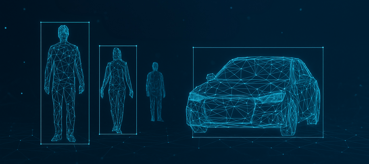
BlogMay 29, 2025
Simplifying Model and Pipeline Deployment with the Voyager SDK
Axelera AI’s A-Tang Fan and Doug Watt explain how the Voyager SDK simplifies the complex task of deploying AI-powered video pipelines on edge devices. This blog explores how its model compiler, model builder, and pipeline builder offer flexible integration paths—whether you’re enhancing an existing VMS, building a new edge product, or optimising for performance.Doug Watt | Director of AI Application EngineeringA-Tang Fan | Engineering Manager - Applications, Model Deployment Lead Many real-world vision applications require the use of multiple deep-learning models, combined in sequence or parallel to perform different tasks. For example, outputting regions of people identified by an object detector into parallel models determining age and gender. Or cascading a vehicle detector into a license plate detector, followed by an optical character recognition model to read the plate. These multiple models are usually connected together with a camera to form an end-to-end inferencing pipeline that outputs images, detections and classifications. Application developers use this information to implement use cases such as crowd analysis and automatic issuing of speeding tickets.Implementing video-streaming pipelines efficiently on performance-constrained edge systems is a hard problem to solve, requiring careful partitioning of the pipeline elements across the heterogeneous hardware components available. Edge AI systems often include a host CPU with embedded image-acceleration hardware, one or more AI accelerator cards connected via PCIe (such as Metis) and one or more input devices.The Voyager SDK offers three powerful deployment tools for building Metis-based vision systems: the model compiler, model builder and pipeline builder. Each tool lets you work at a different level of abstraction.The lowest level provides full control over integrating Metis in systems with custom video handling The highest level lets you perform inferencing in applications while abstracting away all complexities of the underlying video pipeline implementation. Together these tools balance control with ease of use, letting you select the development path that most closely matches your system integration requirements. Built from the ground up, the Voyager software stack lets you strike the perfect balance between control and ease of use.Model Compiler: The Traditional ApproachThe Voyager model compiler supports the industry standard approach to AI deployment by compiling from a PyTorch or ONNX model. The compiler automatically quantizes your model for Metis hardware and generates binary code that performs tensor inferencing. You then integrate this code within your host application using the Voyager AxRuntime API.AxRuntime is a Khronos-inspired API, supported in both C/C++ and Python, which provides precision control over:Execution of Metis code either synchronously or asynchronously within an end-to-end application pipeline The use of threading, queues and other low-level embedded programming techniques needed to run pipelines efficiently on hardwareThe application must capture decoded images from a camera in the required color format, then handle pre-processing to prepare images for model input, and any post-processing needed to refine the raw output.One approach is to utilize the PyTorch libraries in your application from training the model, like torchvision resize and crop transformations, along with a library such as OpenCV for decoding H.264 video and converting it to RGB. This usually results in good accuracy, but poor performance on embedded systems due to inefficient sharing of data between the hardware components. An alternative approach is to implement the entire pipeline in a multimedia framework optimized for video streaming and buffer sharing. Axelera provides an integration plugin for the industry-standard GStreamer framework, based on AxRuntime, which integrates Metis inferencing into existing pipelines. GStreamer provides plugins for many image-processing operations, such as resizing and cropping, but requires custom plugin development for many AI-based operations. For example, post-processing a model output to identify overlapping boxes for the same object, cascading object detections into secondary models, and tracking detected objects over time. Moreover, utilizing off-the-shelf plugins for image pre-processing can significantly reduce accuracy of the deployed model unless the GStreamer implementation precisely matches the PyTorch libraries used during model training. See the dangers behind image resizing for a more detailed explanation.Due to the effort required to achieve accurate, high-performance deployments using only the model compiler, it’s typically used to integrate Metis within existing solutions already discussed above, for example an AI-enabled video management system (VMS). Model Builder: The Traditional Approach, EnhancedThe Voyager model builder extends the model compiler with support for pre-processing and post-processing on the host. It outputs a single model executable file optimized for execution on the host CPU with optional image acceleration hardware and one or more Metis devices.Models can be input to the model builder as either ONNX files with both image and tensor operators, or as YAML files that reference a PyTorch model and list its pre-processing and post-processing operations declaratively. These operators are implemented in a Voyager computing kernel library, runnable on the host, with support for image accelerators such as Intel UHD Graphics (via VA-API) and ARM Mali (via OpenCL). The deployed model executable is then run with a single call to AxInferenceNet (part of the AxRuntime API), which internally pipelines the image and tensor operations across the available hardware as efficiently as possible. AxInferenceNet is supported in C/C++, with Python support to follow. It builds upon AxRuntime with additional optimizations that:Allocate buffers to meet the alignment requirements of the hardware that executes the upstream and downstream elements Utilize mechanisms such as dma-buf to share buffers for DMA access, and interoperability extensions such as cl_khr_external_memory_dma_buf to map shared memory between hardware components without copying buffers Fuse together adjacent pipeline elements running on the same hardware component. For example, combining scaling, normalization and quantization into a single compute kernel to avoid generating intermediate data, minimizing compute and bandwidth requirements In your application code, you can simply connect multiple AxInferenceNet elements together to construct more complex multi-model pipelines. The resulting pipeline can be integrated either directly with your application code (when using OpenCV, for example) or as part of a dedicated GStreamer pipeline using the Axelera integration plugin.AxInferenceNet reduces the development effort needed to achieve accurate and performant model deployments while retaining control and flexibility over the construction and use of end-to-end pipelines within your application. It’s particularly useful for cases where the end-to-end video pipeline is already implemented, and where application-level fine-tuning is required. For example, when implementing an inferencing server or video management system that dynamically processes many streams and models. Pipeline Builder: Application Development, ReimaginedThe Voyager pipeline builder offers the highest level of abstraction: Describe your complete AI-based computer vision pipeline declaratively, at a high level, within a single YAML configuration file, and, Deploy and utilize the pipeline directly from within your application, without needing to consider low-level implementation details for your target hardware. A YAML pipeline may include the following tasks:Conventional image pre-processing operations such as perspective transformations, denoising, low-light enhancement and color space conversion Model pre-processing operations such as resizing, scaling, cropping, letterboxing, normalization and tensor conversion Neural networks such as object detection, key-point detection and segmentation Post-processing operations such as tensor decoding, non-maximal suppression (NMS) and region of interest (ROI) extraction Cascading the output of one model as input to a secondary model. For example, outputting the ROI of a detected car into a secondary license plate detector Running multiple models in parallel. For example, to detect attributes such as a person’s gender, age and ethnicity Tracking detected objects over time. For example, based on the distance between ROIs in consecutive frames or using re-identification techniquesThe pipeline builder deploys YAML files optimally across the hardware components available on the target system. Building upon AxRuntime and AxInferenceNet, it abstracts away all details of the low-level implementation such as connecting multiple models together, connecting the pipeline to one or more camera sources, and efficiently scheduling pipeline execution in parallel with the application code.In your application code, simply declare an InferenceStream object (in either C/C++ or Python), connect the stream to one or more input devices (cameras, video files, etc.), and then iterate to obtain images and inference metadata. Voyager provides additional libraries for analyzing and visualizing inference metadata within your application.InferenceStream objects support numerous advanced features and configuration options, which traditionally required the use of a fully-fledged video management system. These features are summarized in the table below. Feature Benefit Example usage Just-in-time optimization of pipeline, based on I/O devices connected in the application Deploy a pipeline once, and use anywhere Maximize runtime performance for any I/O configuration Input video from different RTSP cameras, USB cameras and file-based workflows Dynamic stream management Run-time scalability: Add and remove video streams from a pipeline on-the-fly without needing to pause and restart the pipeline Applications that dynamically change camera feeds Dynamic model management Run-time flexibility: Switch models used to analyze a stream on-the-fly without needing to pause and restart the pipeline Applications that dynamically change models. For example, based on the scene Per-stream configuration Apply different tailored parameters to the pre-processing elements of each stream Applications processing multiple camera streams with different calibration settings. E.g. perspective transformations and rotations Fault-tolerant operation Pipeline maintains functionality when individual channels experience outages, with automatic recovery when signals are restored IP cameras operating in poor networking conditions Adaptive frame processing Maintains consistent performance through selective dropping and interpolation techniques Avoids queues from filling up leading to increased latency or lag Record each incoming 4K stream at native 30fps while analyzing it at only 10fps Dynamically adjust the number of ROIs processed in a cascaded pipeline to keep up with the incoming frame rate while processing as much of a scene as possible (e.g. when analyzing a large crowd) Pipelines configured using InferenceStream objects can be rapidly re-configured to enable or disable the above features and fine-tuning parameters, all from within your application. In this way, Voyager allows you to focus on utilizing the results of AI inferencing to develop your business use cases while ignoring the complexities of optimizing video processing on the target hardware. Selecting the Most Suitable Development PathWith Voyager SDK, you select the development path that most closely meets your development and integration requirements. The table below provides a few common scenarios. Example scenario Recommended deployment tool and integration API Reason for recommendation Develop a new edge-based vision product, or upgrade an existing product to support AI inferencing use cases Pipeline builder with InferenceStream Invest your time in creating business value by differentiating your product with AI analytics (rather than spending time on embedded programming and performance optimization) Integrate AI processing into existing vision products based on frameworks such as GStreamer or OpenCV Model builder with AxInferenceNet Re-use as much of your existing video-processing pipeline as possible Easily “plug-in” models to your pipeline with minimal code changes while achieving good performance Add AI analytics to an existing VMS with its own video handling Model compiler with AxRuntime The VMS may contain existing software infrastructure for video decoding and image processing that needs to be used in the product Supporting The CommunityOur goal with the Voyager SDK is to make AI development accessible to everyone, by providing robust and flexible tooling that meets the demands of real-world production deployments, and your feedback is essential in helping us achieve this goal. Feel free to start a post on the Axelera AI community telling us how you’re using our tools, what works well and what you’d like to see improved — such as adding support for different image accelerators, image pre-processing tasks, models or media streaming frameworks — to help you develop and integrate AI inferencing within your applications. We’re here to listen, improve, and unlock the full potential of AI at the edge together.
Related products:AI Software
BlogApr 16, 2025
Momentum and Milestones: Axelera AI’s Progress in a Changing World
The world has been chaotic lately - market swings, tariffs, companies being acquired (Kinara by NXP), other companies are refusing acquisition (Furiosa allegedly declined an $800m buyout from Meta), DeepSeek made everyone question the future of closed AI models and model scaling, while OpenAI’s Sam Altman committed to an “open-weight” AI model to come out this summer - something no one thought would happen.As I was reflecting on all of these, and Axelera’s state in it all, I find myself incredibly grateful.Despite everything happening around us, our team has been focusing on what we can control: solving customer problems, building world-class technology, and partnering with some of the world’s best technology providers. So much to be thankful for, and I want to share some of these reasons with you.We have seen amazing progress towards our vision of bringing artificial intelligence to everyone, to truly democratize what could be the most revolutionary technology we have seen in our lifetime.I am proud to share the latest milestones as we continue to drive innovation, growth, and the democratization of AI. The milestones can be divided in 5 main categories:Product & Commercial traction Funding Partnerships Democratization of our technology Supporting Europe’s audacious sovereign initiatives Product & Commercial traction Our first products, the Metis AIPU and the Voyager SDK are both shipping to customers in production, and companies or developers wanting to test can now purchase from our very own webstore and get the hardware in their hands in a matter of days. We also published the Voyager SDK on GitHub, launched our Model Zoo.We recently launched our AI single-board computer which integrates in the same board a powerful RockChip 3588 with our Metis™ AI processing unit: you can get a high-end edge AI computer with 210 TOPs AI computing power in a standard mini-ITX form-factor! You can pre-order at special discounted price!We are also preparing for the launch of a powerful PCI-e card with 4 Metis™ AI processing units. Stay tuned for the pre-order announcement.Customers like duagon have demonstrated with us at Embedded World to showcase how our Metis product, paired with their industrial solutions, can help improve railway operations.We are continuing to partner with the channel ecosystem too and are proud to be working with Azulle and Arcobel, and look forward to more announcements in this space soon.Order directly from the Axelera AI storeFundingAxelera AI recently secured up to €61.6 million in funding from the EuroHPC Joint Undertaking and member states to develop Titania™, a high-performance, energy-efficient, and scalable AI inference chiplet. This funding, part of the Digital Autonomy with RISC-V for Europe (DARE) Project, will support the development of a very high-performance, high-efficiency chiplets based on Axelera AI's innovative Digital In-Memory Computing (D-IMC) architecture, which enables near-linear scalability from the edge to the cloud.We were selected for the EIC Step Up program which will provide investments of between €10 and €30 million (per company) aiming to leverage private co-investment and achieve financing rounds of €50 to €150 million or more. What an honor to be selected from the 34 applicants to receive this additional equity investment!With this new funding, Axelera AI has raised over $225 million USD in just three years, further solidifying our position as a leader in AI hardware acceleration technology.Axelera AI secures grant to develop a scalable AI chipletPartnershipsBetween Embedded World, ISC West, and CES, we have been proud to showcase our work with partners like SeeChange, Lenovo, Dell, Aetina, Advantech, Seco, Duagon, and many others!We recently demonstrated running real-time analytics on an 8k video stream. When we took this demo to ISC West, I was reminded of how our industry-standard form factor approach is helping make integration simple for customers. The quick story is our demo systems were caught in US customs coming from Amsterdam – not for tariffs 😉- so the team purchased a gaming PC off the shelf in Las Vegas, borrowed some 8K cameras from our friends at Axis, and were able to showcase the powerful capabilities of Metis! For more details, please see the blog.At the Embedded World in Nuremberg, duagon and Axelera AI showcased two pre-series products with integrated Metis™ AIPUs, highlighting the potential of high-performance AI applications at the embedded level. The AIPU modules, which leverage digital in-memory computing power, deliver exceptional performance per watt for inference workloads, making them ideal for parallel processing of visual information. The two products, the Box PC BL74A and the CompactPCI card G506A, are now entering the test phase and will be available as standard products with embedded AI capabilities once certified.One other to highlight is the recent announcement with the European Space Agency to bring its Metis inference acceleration platforms to space, supporting the ESA's mission to protect the planet, explore the universe, and strengthen European autonomy. The partnership will enable the ESA to leverage Axelera's sovereign technology and long-term availability to deliver high-performance and low-power AI capabilities in space, supporting missions that may last for years or even decades. This collaboration marks an exciting step forward in the intersection of AI and space exploration, empowering scientists to answer some of the universe's biggest mysteries.We were also delighted to see Thales in France showcase what they are doing with Metis as they are working to keep humans in the loop of their AI solutions.Metis in space Democratization of AI with AxeleraAxelera AI has furthered its strategy to democratize artificial intelligence everywhere through a strategic partnership with Arduino, the global leader in open-source hardware and software. The collaboration combines Axelera AI's Metis™ AI Platform with Arduino's Portenta to provide customers with easy-to-use hardware and software solutions for AI innovation. This partnership enables users to dictate their own AI journey with tools that deliver high performance and usability at a fraction of the cost and power of other solutions available today. Arduino is one of the world’s largest sources of hardware and software for hardware and software developers. Arduino has a massive user base of over 30 million registered users worldwide. This community of innovators has created an astonishing 100,000+ projects on the Arduino platform, ranging from simple circuits to complex robotics, AI, and IoT devices. Additionally, Arduino has sold over 20 million boards, a testament to the platform's popularity and versatility. This partnership will truly democratize our technology.Additionally, Axelera’s technology is now also available for purchase online. Yes, we opened our very own online store. What does a full-fledged Axelera customer experience look like? Well, customers can download our Voyager SDK and read SW docs. They can buy our boards and systems with one mouse click, and then get support and documentation while interacting with other developers right here on the Axelera AI Community. To date we have shipped to a dozen countries and are looking forward to hearing how these developers use their Metis systems!Metis and Portenta, together Supporting Europe Technology SovereigntyIn addition to partnering with the EuroHPC and the DARE project, Axelera has been invited to participate in a number of incredibly important discussions to advance the European technology landscape. We are proud to participate and share our expertise with the governments of France through the AI Action Summit, the Netherlands at the State of Dutch Tech, and across Europe through the D9+. Most recently, I was honored and humbled to participate in the launch of the AI Continent Action Plan in Brussels.It was a great discussion, full of valuable insights that make me genuinely optimistic about the future of European technology. A few key takeaways:With the first AI Factories already operational, and the launch of the AI Gigafactories call for interest, Europe is showing that when we work together, we can move fast and decisively. Across many parts of the AI value chain, Europe has players delivering cutting-edge solutions. With stronger collaboration and vertical integration — from hardware to applications — European AI can win in key sectors. European leaders increasingly recognize the importance of stimulating demand for “‘made in Europe” products, both in public procurement and beyond. Europe has plenty of capital. Now is the time to unleash it and direct it towards strategic sectors like AI and deep tech. The European defense market is becoming a strategic growth driver for our deep tech sector. Many EuroHPC Joint Undertaking (EuroHPC JU) centers are open to testing and deploying experimental European hardware and software solutions, helping our deep tech startups scale. They are also giving startups simplified access to their infrastructure, which is strategic to compete with well-funded overseas companies A true European single market is essential to build the first European trillion-euro company.The combination of all of the discussions makes me incredibly excited. The current global turmoil has served as a wake-up call for Europe, and we are standing united to be successful. SummaryIn a recent all company meeting, I told all employees that ‘the best is yet to come’. As I look back on the past period, I'm pleased to say that we've successfully set up our chess pieces on the board. We've made strategic moves to position ourselves for success, and our team is now well-equipped to make the most of the opportunities ahead. Just as a chess player must carefully plan their opening moves to set themselves up for checkmate, we've taken the time to lay the groundwork for our future growth and success. With our pieces in place, we're now poised to make the moves that will take us to the next level.It’s still day one, the best is yet to come!
Related products:IndustryCompany
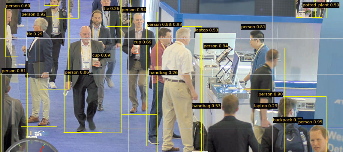
BlogApr 4, 2025
Outperforming the AI Crowd at ISC West with 8K YOLOv8l on the Edge
What happens when you take one of the most demanding computer vision models, push it to 8K resolution, and run it live on the edge—right in the middle of the world’s biggest security tech trade show? At ISC West 2025, that’s exactly what we did. Here’s how.Just a few months ago at CES I was speaking with a nationwide retailer in the process of upgrading its store camera systems to 4K. We discussed its AI strategy given that many state-of-the-art models are still trained at HD resolutions or less. Reasons for this are that training at higher resolutions is more computationally expensive, and labelling high-resolution datasets is resource intensive. Yet the point of inferencing at high resolution is often just to increase the distance from the camera at which objects can be detected, and not anything related to the model’s fundamental accuracy. How We Cracked High-Resolution Inferencing at the EdgeWith conventional inferencing, high-resolution video is downsized to the native model input resolution, producing a loss of information prior to inferencing. Tiling techniques such as SAHI mitigate this loss by subdividing each input image into a grid, running the model on each tile individually, and then reconstructing all detections with respect to their position in the original image.A key Axelera AI differentiator is the ability to rapidly and efficiently scale up inferencing by using multiple cores and chips. So we decided to showcase the popular, yet computationally-demanding, YOLOv8l model running on Metis with an IP camera at 8K resolution. Developing this capability – not just for demo but as a general-purpose SDK feature that anyone can use with their own models – is technically quite challenging. YOLOv8l is a large model with 43.7M parameters compared to the industry benchmark SSD-MobileNetv2, which has 3.4M parameters. It can take over 100 times longer to run, even before tiling. YOLOv8l’s native input size is 640x640, which subdivides an input video at 8K resolution (7680x4320) into a grid of 12x7 tiles, allowing for some vertical overlapping. In addition, to ensure accurate detection of objects spanning multiple tiles, the original, downsized image is also used as a model input, for a total of 85 parallel streams. This processing must be split efficiently end-to-end between the host processor and Metis accelerator, with the host preparing vast amounts of camera data for inferencing Tasks include:Color conversion Scaling Letterboxing Tensor conversion Post-processing The latter of these applies algorithms such as non-maximal suppression to the output, removing duplicate detections between tiles.Live feed from the 8K camera with real-time object detection. A lot of it!Real-World Deployment, Real-World ResultsFor the ISC West demo, we placed an 8K camera four meters above our booth - huge thank you to Axis who loaned us a Q1809-LE 8K bullet camera when ours got stuck with US Customs. From there, it could survey a section of the convention center floor, accurately reflecting how these cameras are actually being deployed in venues, stadiums, airports and more.At this distance we found the optimal tile size to be 1280x1280, with each tile capturing a range of people and objects on the show floor. Using an Intel Core i9-based PC and two Metis cards, we were able to detect objects accurately with YOLOv8l at a rate of 23 frames/second. This equates to processing around 300 1280x1280 tiles per second. Moving to the smaller, but still very capable YOLOv8s model enables the same levels of performance using only a single Metis device, while our upcoming 4-chip PCIe card enables the highest levels of accuracy and performance. The ability to easily change models and parameters using our Voyager SDK, simply by modifying YAML configuration files, makes it incredibly easy to build powerful systems for processing multiple high-definition camera streams at low latency and high frame rates. It’s also testament to the flexibility that has come from building the Voyager SDK from the ground up to deliver ease of use and high performance at the same time, all within a single development environment. Building our SDK foundations to enable this degree of flexibility was not, however, such an easy problem to solve.Axelera AI Metis In actionA Challenge in the MakingMy journey with heterogeneous computing began a decade ago at GPU IP-supplier Imagination Technologies, where I worked with mobile OEMs trying to repurpose their GPUs for emerging compute workloads in the Android market. At this time, the use of GPU computing in application processors was still in its infancy. Apple, as Imagination’s lead customer, was developing in-house features for the iPhone, and a fragmented Android ecosystem struggled to find compelling use cases in phones and tablets. Through various industry collaborations we did eventually achieve a few Android deployments, most notably (or perhaps notoriously) real-time camera “beautification.” But my feeling at that time was that embedded GPU computing was failing to reach its full potential, in part due to the difficulties of programming heterogeneous systems-on-chips using low-level APIs.Fast forward to the last couple of years and we’re now in the midst of a major industry shift: the transitioning of compute from cloud data centers to edge devices, bringing end-user benefits such as reduced latency, enhanced privacy and lower costs. With AI playing an increasingly important role in products everywhere, many companies are looking to incorporate AI accelerators into their edge products.Many of these products are already designed using host processors with embedded GPUs that offer impressive image processing capabilities. However, when it comes to integrating these capabilities within end-to-end AI pipelines, the state of the industry has unfortunately moved towards proprietary solutions. Apple has orphaned OpenCL in favour of its Metal API, which, albeit very capable, is proprietary to Mac. NVIDIA’s ecosystem is firmly rooted in CUDA, also a proprietary API. At the same time, open APIs such as Khronos’s Vulkan has not yet delivered on its promise to evolve from a graphics-centric API to one that unifies compute-based kernels.Against this backdrop, we set out to develop an SDK that makes it easy to integrate Metis AI accelerators with a wide range of host processors, while maximizing end-to-end performance by leveraging the image-acceleration APIs available on these hosts. This challenge was just one part, albeit an important part, of the broader Axelera AI vision to make artificial intelligence accessible to everyone.This is the 8K camera in position at the Axelera AI ISC West boothFirst Make it Easy to UseWe started by making it easy for developers to express their complete AI inferencing pipeline in a single YAML configuration file. Pipelines are described declaratively, including all preprocessing and post-processing elements, and optionally combining multiple models in parallel or sequence so that, for example, the output of a person detector is input to a secondary weapon detector. We created YAML files for every model in our model zoo, using weights trained on default industry-standard datasets, and we made it easy to customize these models with pre-trained weights and datasets. We then developed a pipeline builder that automatically converts these YAML definitions into functionally-equivalent low-level implementations for a range of target platforms. We designed high-level Python and C/C++ application integration APIs that enable developers to dynamically configure these pipelines at runtime with mixtures of different video sources, formats and tile sizes. At the application level, developers can simply iterate to obtain images and inference metadata, which can then be analyzed and visualized using Voyager application libraries. The Voyager SDK provides a single environment in which pipeline development and evaluation can proceed hand-in-hand with application development, from product ideation all the way through to production. Then Optimize, RelentlesslyWorking closely with early access customers, we prioritized the optimizations that mattered most to their use cases, like adding support for Intel Core hosts with VAAPI-accelerated graphics and Rockchip ARM platforms with OpenCL-accelerated Mali GPUs. Integrating these compute APIs with other hardware, such as video decoders and the Metis PCIe driver, required careful consideration of various low-level issues, such as alignment requirements when allocating memory, and understanding which API interoperability extensions were supported most efficiently and reliably by the different hardware vendors. This was codified into our pipeline builder so that it can construct efficient zero-copy pipelines that pass only pointers between elements. Unnecessarily copying even a single buffer can substantially degrade performance on bandwidth-constrained devices, so a lot of time was spent considering optimal approaches for different combinations of tasks and devices. With the core framework in place, we added optimization passes to the pipeline builder that fuse together different combinations of pre-processing tasks on the same device. This eliminates unnecessary generation of intermediate pipeline data that isn’t required by the application, saving additional memory bandwidth. Over time the pipeline builder has matured into a product that can generate near-optimal implementations of many complex pipelines to meet the demands of real-world applications, and we’re excited to make it available to our broader community.Surveying the competitive landscape with our high-resolution 8K inferencing capabilitiesWhere We’re Headed NextThe first public release of the Voyager SDK is a major milestone on a journey that offers many exciting opportunities. As part of this first release we’ve also opened up lower-level APIs on which the pipeline builder and application integration APIs are built. These include a Khronos-inspired low-level AxRuntime API (available today in C/C++ and Python), which provides full control over all hardware resources used to build end-to-end pipelines.There’s also a mid-level AxInferenceNet API (available today in C/C++ with Python to follow) that allows direct control of model execution from within an application (distinct from our highest-level API that fully abstracts pipelines to objects generating images and metadata). We’re excited to see how developers make use of these APIs, and how they would like to see them further improved. Feel free to share any such feature requests.As developers continue to push the boundaries of what’s possible with AI, Axelera AI continues to innovate and ensure the broadest adoption of our products. For example, developers working with high-resolution cameras often need to manage large amounts of data within their application, from capturing and recording video in real-time, to scanning complex scenes over time to track, identify and analyze objects, and detecting key events in dynamic, real-world environments. These are fundamentally difficult problems to solve, but by building tools that keep raising the abstraction level at which developers can create applications, I believe Axelera AI is perfectly positioned to deliver on the promise of making AI accessible to everyone.
Related products:AI Software
BlogMar 28, 2025
Voyager SDK is Available Now on GitHub
The importance of software for unlocking the value of artificial intelligence cannot be overstated: the most powerful hardware in the world is just a paperweight without a usable software stack. At Axelera AI we’ve built the Voyager Software Development Kit (SDK) to give developers and ML engineers a simple solution for developing and deploying AI. Today, we’re excited to share that the Voyager SDK is now publicly available on our GitHub page. IntroductionThe Voyager SDK is an end-to-end integrated software stack for Axelera AI’s inference platform which has been designed for performance, efficiency and ease of use. It enables developers to deploy pre-trained machine learning (ML) models, and to construct end-to-end optimized application pipelines quickly and easily. Whether you have trained your own model weights, are using an open source model with pre-trained weights, or want to build on one of the models offered in our model zoo, Voyager provides an effortless path to deploy and evaluate a model on Axelera AI’s hardware platforms, to build an inference pipeline using it and to integrate the pipeline into your application logic.Voyager SDK offers a development environment where the developer deploys a model, measures its accuracy and performance and integrates it into an application pipeline. It also offers a runtime environment (i.e., a runtime stack) that offloads the execution of the pipeline when the application runs on an edge system. The two environments are logically separate but can also co-exist on the same system. What is included in Voyager SDK?We distribute the latest version of the Voyager SDK as a GitHub repository which,among other content, offers the following:An automated installer for the core binary packages of the SDK, including native packages and Python wheels. For certain packages, such as the Linux kernel driver, native source code is available as well. The installer can be used to install the developer environment, the runtime environment or both. Source code for the AI pipeline builder, image acceleration libraries, GStreamer plug-ins, inference server and model evaluation infrastructure. Comprehensive documentation to support developers using our platform. Our documentation covers general topics such as installation, getting started and performance benchmarking, as well as tutorials on more specific topics such as deployment of custom model weights. Additional documents specific to various host platforms and upgrade instructions will be available in our customer portal. A model zoo of optimized models, including dozens of models for tasks such as image classification, object detection, semantic segmentation, instance segmentation and keypoint detection. As we optimize the performance and accuracy of new models, our model zoo will be expanding continuously with additional models and use cases. Multiple sample pipelines and applications that exemplify the use of our stack and can help streamline development and speed up time-to-market.Performance Recently we published a blog post on the performance and accuracy achieved with benchmark computer vision models on Metis AI processing units. Those tests were run using the software we are releasing today, so you can reproduce those benchmarks for yourself and, more importantly, take advantage of the performance of Metis in your applications. For the latest benchmarks and performance numbers, please visit here. Why Now?Axelera AI was founded on the principle that everyone should have access to leading edge inference capabilities. We believe openness is the best way to empower developers and we are thrilled to have reached this milestone. For over six months our customers have been using Voyager, providing us feedback, and helping shape our roadmap. We look forward to now broadening both the access and the feedback through our online community. Interested in Getting Involved?Our team is committed to fostering a collaborative environment by encouraging open source contributions. Developers can submit new pipelines or improvements via pull requests, which will be reviewed and potentially integrated into the repository. With this approach we aspire to enhance the quality and reach of our SDK and build a vibrant community of contributors.Make sure you’re signed up here at the Axelera AI community to discuss your projects, ask questions, and support your fellow developers.Still don’t have a Metis inference accelerator? Get one today.
Related products:AI Software

BlogMar 7, 2025
The Future of AI Inference: Introducing Titania
Evangelos Eleftheriou | CTO at AXELERA AI It is with great enthusiasm and a sense of humble pride that I share a pivotal development in the realm of AI and high-performance computing (HPC). Axelera AI, as part of the esteemed EuroHPC Joint Undertaking (JU) DARE consortium, has embarked on an ambitious journey to revolutionize AI inference technology with our groundbreaking chiplet architecture, Titania. Unveiling TitaniaTitania represents a synthesis of our foundational principles: high performance, low power consumption, and unparalleled scalability. This innovative AI inference chiplet is a testament to the ingenuity and dedication of our team, who have tirelessly worked to bring this vision to life. Built on our proprietary Digital In-Memory Computing (D-IMC) architecture, Titania offers near-linear scalability from the edge to the cloud, marking a significant leap forward in AI computing efficiency. “Our Digital In-Memory Computing (D-IMC) technology leverages a future-proof, scalable multi-AI-core architecture, ensuring unparalleled adaptability and efficiency. Enhanced with proprietary RISC-V vector extensions, this versatile mixed-precision platform is engineered to excel across diverse AI workloads. Uniquely, our architecture facilitates scaling from the edge to the cloud, streamlining expansion and optimizing performance in ways that traditional cloud-to-edge approaches cannot. We are setting a new standard for AI infrastructure, making true scalability a tangible reality”Evangelos Eleftheriou, CTO and Co-Founder, Axelera AI The Significance of TitaniaWhy is Titania so crucial for the future of AI? The answer lies in its design and the pressing needs of our rapidly evolving industry. As AI applications become more sophisticated, models get bigger, and the compute demands seem endless, the technology industry owes it to the world to bring a more efficient, scalable, and cost-effective inference to the market. Titania is engineered to meet these demands, providing server-grade performance with the energy efficiency required at the edge. This balance is essential for applications ranging from weather prediction and industrial automation to security monitoring and advanced Large Language Models with multimodal capabilities.Collaboration and SupportThe development of Titania is made possible through the generous support of the EuroHPC JU and the DARE consortium which have allocated €240 million in funding, of which Axelera AI will receive up to €61.6 million. This support underscores the importance of fostering European innovation and technological sovereignty in the HPC ecosystem. It also aligns perfectly with Axelera AI’s mission to bring state-of-the-art AI capabilities to a broader range of applications and industries. Our Technological Edge At the core of Titania’s capabilities is our D-IMC technology, integrated with cutting-edge RISC-V vector extensions. This combination ensures that our chiplet can handle diverse AI workloads with remarkable efficiency and adaptability. The scalable multi-AI-core architecture sets a new standard for AI infrastructure and streamlines the expansion process, making true scalability a tangible reality. Looking AheadOur journey with Titania is just beginning. We anticipate the first systems powered by Titania to be available by 2027, supporting a vast array of use cases and demonstrating the profound impact of this technology. As we forge ahead, we remain committed to our core values and dedicated to delivering cutting-edge solutions that address the AI industry’s most pressing challenges. A Heartfelt Thank YouI extend my deepest gratitude to the EuroHPC JU, the DARE consortium, and our incredible team at Axelera AI. Their unwavering support and commitment have been instrumental in driving this project forward. Together, we are setting a new benchmark for AI inference technology and paving the way for a future where AI capabilities are more accessible, efficient, and impactful than ever before. Titania is more than just a chiplet; it represents the culmination of years of research, innovation, and collaboration. It embodies our vision for the future of AI and our dedication to pushing the boundaries of what is possible. I invite you to join us on this exciting journey as we continue to explore new frontiers in AI and HPC.
Related products:AI AcceleratorsTechnology
BlogFeb 19, 2025
Why Metis Outperforms Competitors up to 5x in Benchmarks (Hint: Software Matters)
Manuel Botija | Head of Product at AXELERA AI Ioannis Koltsidas | VP AI Software at AXELERA AI Exec Summary: The Metis AI Processing Unit (AIPU) is an inference-optimized accelerator for the Edge. We are proud to showcase up to a 5x performance boost over competitive accelerators in terms of raw inference performance for key families of Neural Networks for Computer Vision along with state-of-the-art accuracy. As significant as 5x is though, we believe the best measurement of performance is application-level performance which is a much better proxy for what the user will realize. For example, if the AIPU can infer that a cat is a cat at 900fps, but the post-processing slows it down so significantly that the user only sees 20fps, the 900fps is nearly useless. Thanks to our easy-to-use Voyager™ SDK, which optimizes the entire data pipeline, we also showcase that Axelera AI’s application performance brings worldclass speed to computer vision applications. Three years ago we started Axelera AI with a singular mission, to empower everyone with the best performance for AI inference. Since then, we have taped-out 3 chips, built the Voyager SDK, and are fulfilling that promise.Today we are pleased to release the latest performance benchmarks based on the upcoming public release of our Voyager SDK, which will be available via our Github repo in March. All of the data measured has been done on our products, within our labs. Competitor data has been utilized from their own published sources as noted below.Multiple Metis AI processing units. The AI chips that accelerate deep learning at the edge Performance Results: Metis vs. CompetitionWhen compared to other AI accelerators, Metis consistently outperforms in key benchmarks such as Ultralytics YOLO models. The chart and table below show the frames per second (FPS) processed by Metis, compared to the throughput of other AI accelerators.This is just some of the benchmarks we have tested and a few of the more than 50 models available for immediate use within our Model Zoo. Software is extremely important to us at Axelera AI and we invest significant resources in ensuring we are always improving. We continue to add optimized models and capabilities to ease development and integration within AI pipelines. Having the highest performance only matters if the users can trust the accuracy of the inference being performed. We are thrilled to say that, thanks to the mixed precision architecture of Metis and the quantization capabilities of our SDK, the achieved accuracy is state of the art.In the following table we list the accuracy measured for various models when running on a machine with full numerical precision (32-bit Floating Point arithmetic, a.k.a. ‘FP32’) and compare it with the accuracy of the same models running on Metis after being quantized by the Voyager SDK. As you can see, the accuracy reduction with Metis is negligible in many cases. Our software team continues to work on optimizations and will keep updates in our public release.Voyager SDKWithout a robust and easy to use software stack, AI hardware is useless. There, we said it! So, to ensure developers can get the most out of our performance-leading hardware, we built the Voyager™ SDK which facilitates the development of high-performance applications. Developers can build their computer vision pipelines using a straightforward, high-level declarative language, YAML. A Voyager pipeline may include one or more neural networks along with their associated pre- and post-processing tasks, which can include complex image processing operations. The SDK automatically compiles, optimizes, and deploys the entire pipeline. While the neural network runs on the Metis AI Processing Unit (AIPU), the SDK also generates code for the non-neural operations of the pipeline, such as image preprocessing and inference post-processing, to take advantage of the host hardware acceleration offered by the host CPU, integrated GPU or media accelerator. Additionally, thanks to the architecture of our chip, the developer can choose how to allocate Digital In-Memory Compute (D-IMC) cores to the application: if there are multiple models, the cores can be loaded in parallel, or they can be cascaded, the decision is yours. This means if you have a very compute heavy model that you want to utilize 3 of the 4 cores to compute, you may. Likewise, if you have four models you want to run in parallel, that is also possible. Application-level performanceRunning a Computer Vision application is much more than just running inference. At Axelera AI we believe it’s important to understand what the realized performance is – meaning, how long does it take to get the answer a user is looking for, that’s the full end-to-end measurement. The Axelera AI Voyager SDK helps optimize the entire data pipeline, including the parts that run on the host CPU or embedded GPU. Why does this matter? This means that both the developer and the users will have a better experience because the SDK will handle the work for the developer, and the user gets faster results.As can be appreciated in the table, Voyager SDK manages to deliver the raw inference performance to the end-to-end application: by optimizing the execution of non-neural operations in the computer vision pipeline we ensure that the application can take full advantage of the unmatched capabilities of Metis.The Voyager SDK is compatible with a variety of host architectures and platforms to accommodate different application environments. Additionally, the SDK allows embedding a pipeline into an inference service, providing various preconfigured solutions for use cases ranging from fully embedded applications to distributed processing of multiple 4K streams. State-of-the-Art Digital In-Memory ComputingWhy is Metis so powerful? One of the key innovations that sets Metis apart from its competition is its use of Digital In-Memory Computing (D-IMC) technology. D-IMC allows for the simultaneous processing and storage of data within memory cells, allowing extremely high throughput and power efficient matrix-vector-multiplication. This approach is particularly beneficial for AI workloads, which require high-speed data access and intensive computation, and all with an average power consumption below 10 watts! i Metis performance was measured on a system equipped with a 13th gen. Intel Core i5 (i5-13600) CPU and a Metis PCIe card, running Ubuntu 22.04 and the production Voyager SDK (v1.2.0). ii https://hailo.ai/products/hailo-software/model-explorer/ as of 2025-02-1
Related products:AI AcceleratorsIndustry

BlogSep 21, 2024
Using oneAPI Construction Kit to Enable Open Standards Programming for the Metis AIPU
Manuel Mohr | Staff Software Engineer at AXELERA AI Open standards enable developers to more easily harness the power of AI accelerators, especially in heterogenous computing. Here you can read in detail why and how we implemented OpenCL using the oneAPI construction kit on Metis.The Necessity of Dedicated AI Hardware AcceleratorsAI applications have an endless hunger for computational power. Currently, increasing the sizes of the models and cranking up the number of parameters has not quite yet reached the point of diminishing returns. Thus, the ever growing models still yield better performance than their predecessors.At the same time, new areas for application of AI tools are explored and discovered almost daily. Hence, building dedicated AI hardware accelerators is extremely attractive. In some situations it is even a necessity, as it enables running more powerful AI applications while using less energy on cheaper hardware. Welcome to the Hardware JungleSuch specialized accelerator hardware poses great challenges to software developers, as they instantly transform a regular computer into a heterogeneous supercomputer, where the accelerator is distinctly different from the host processor. Moreover, each accelerator is different in its own way and wants to be programmed appropriately to actually reap the potential performance and efficiency benefits.In his 2011 article*, Herb Sutter heralded this age with the words “welcome to the hardware jungle”. And since he wrote this article, a thick jungle it has indeed become, with multiple specialized hardware accelerators now being commonplace across all device categories ranging from low-end phones to high-end servers.So what’s the machete that developers can use to make their way through this jungle without getting lost? Why Custom AcceleratorIinterfaces Are a Bad IdeaThe answer lies in the creation of a suitable programming interface for those accelerators. Creating a custom interface that is completely tailored for a new accelerator silicon could let a developer exploit every little feature that the hardware has to offer to achieve maximum performance.However, upon closer inspection, this is a bad idea for a variety of reasons. Firstly, while there might be the possibility of achieving peak performance with a custom interface, it would require expertise that is already hard to come by for existing devices and even rarer for new devices. The necessary developer training is time-intensive and costly.Even more importantly, using a different bespoke interface to program each accelerator can also result in vendor lock-in if the created software completely relies on such a custom interface, making it highly challenging and significantly more expensive to switch to a different hardware accelerator. The choice of programming interface is thus crucial not only from a technical perspective, but also from a business standpoint. At Axelera, we therefore believe that the answer to the question of how to best bushwhack through the accelerator jungle is to embrace open standards, such as OpenCL* and SYCL*4. Open Standards for Open InteractionOpenCL and SYCL are open standards defined by the Khronos Group. They define an application programming interface (API) for interacting with all kinds of devices, as well as programming languages for implementing compute kernels to run on these devices.SYCL provides high-level programming concepts for heterogeneous computing architectures, together with the ability to maintain code for host and device inside a shared source file.But providing a standard-conformant implementation of such open standards poses a daunting challenge for creators of new hardware accelerators. The OpenCL API consists of more than 100 functions and OpenCL C specifies over 10000 built-in functions that compute kernels can use. It would be great if these open standards were also accompanied by high-quality open-source implementations that are easy to port to new silicon. Fortunately, in the case of OpenCL and SYCL, this is indeed the case. Increased Developer ProductivityOpen standards such as OpenCL & SYCL promise portability across different hardware devices and also foster collaboration and code reuse. After all, it suddenly becomes possible and worthwhile to create optimized libraries that are usable for many devices, which ultimately increases developer productivity.Axelera is a member of the UXL Foundation*, a group that governs optimized libraries implemented using SYCL. These libraries are compatible with this software stack, offering math and AI operations through standard APIs. Conquering the Jungle with the oneAPI Construction KitThe open source oneAPI Construction Kit from Codeplay is a collection of high-quality implementations of open standards, such as OpenCL and Vulkan Compute, that are designed from the ground up to be easily portable to new hardware targets. We want to share our experiences using the Construction Kit to unlock OpenCL and SYCL for our Metis AI Processing Unit (AIPU)*. Prerequisites for deployment In order to enable porting an existing OpenCL implementation to a new device, two prerequisites must be fulfilled: There must be a compiler backend able to generate code for the device’s compute units. As the oneAPI construction kit, like virtually all OpenCL implementations, is based on the LLVM compiler framework, in this case this means having an LLVM code generator backend for the target instruction set architecture (ISA). As our Metis AIPU’s compute units are based on the RISC-V ISA, we could just use the RISC-V backend that’s part of the upstream LLVM distribution to get us started. If the accelerator uses a non-standard ISA, an adapted version of LLVM with a custom backend can of course be used with the Construction Kit as well. There must be some way for low-level interaction with the device, to perform actions like reading or writing device memory, or triggering the execution of a newly loaded piece of machine code. As we already supported another API before looking into OpenCL, such a fundamental library was already in place. In our case, it was a kernel driver exposing the minimal needed functionality to user space (essentially handling interrupts and providing access to device memory), accompanied by a very thin user space library wrapping those exposed primitives.Implementing HALWith these prerequisites being met, we started following the Construction Kit’s documentation*. The first thing to do is implementing what the Construction Kit calls the “hardware abstraction layer” (HAL). The HAL comprises a minimal interface that covers the second item of the above list and consists of just eight functions: allocating/freeing device memory, reading/writing device memory, loading/freeing programs on the device, and finding/executing a kernel contained in an already loaded program.In order to avoid having to deal with the full complexity of OpenCL from the get-go, a smaller helper library called “clik” is provided by the Construction Kit to implement the HAL. This library is essentially a severely stripped-down version of OpenCL, with some especially complex parts like on-line kernel compilation being completely absent. Hence, the clik library serves as a stepping stone for getting the HAL implemented function by function, and provides matching test cases to ensure that the HAL implementation fulfills the contract expected by the Construction Kit. After all tests pass, this scaffolding can be removed, and the resulting HAL implementation can be used to bring up a full OpenCL implementation.In our case, implementing the HAL was straightforward. The tests enabled a quick development cycle, where more tests started passing every time some new functionality was added or pointed out problems where the HAL implementation didn’t meet the Construction Kit’s expectations. In total, it took about two weeks of full-time work by one developer without prior Construction Kit knowledge to go from starting the work to passing all clik tests. Configuring a complete OpenCL stack.After gaining confidence that the Metis HAL implementation was functional, we could continue with the next step and bring up a complete OpenCL stack* . This, too, was surprisingly quick, taking roughly another two person weeks of developer time. The Construction Kit again provides an extensive unit test suite, whose tests can be used to guide development by pointing out specific areas that aren’t working yet.All bring-up work was initially performed using an internal simulator environment, but after passing all tests there, we could quickly move to working on actual silicon (see 8). As the first real-world litmus test for our Metis OpenCL implementation, we picked an OpenCL C kernel that is currently used for preprocessing as part of our production vision pipeline. By default, the kernel is offloaded to the host’s GPU. However, with Metis now being a possible offloading target for OpenCL workloads as well, we pointed the existing host application at our Metis OpenCL library and gave it a try. We were very happy to see that without any modifications to the host application1, we were able to run the vision pipeline while offloading the computations to Metis instead of the host GPU. In total, with the transition to actual silicon taking another week of developer time, it took us around five person weeks of development effort to go from having no OpenCL support to having a prototype implementation capable of offloading an existing OpenCL C kernel used in a production setting to our accelerator.Hence, in our experience, OpenCL and the oneAPI Construction Kit fully delivered on the promises of easy portability and avoiding vendor lock-in.Opening up PossibilitiesHaving a functional OpenCL implementation is also an important building block that opens up many other possibilities. OpenCL can be used as a backend for the DPC++ SYCL implementation*, which enables a more modern single-source style for programming accelerators.Even more importantly, a SYCL implementation makes it possible to tap into the wider SYCL ecosystem. This includes optimized libraries, such as portBLAS* providing linear algebra routines and portDNN* providing neural-network-related routines, but also brings the potential to support the UXL Foundation libraries including oneMKL*, oneDPL*, and oneDNN*. Alongside these libraries it also includes tools like SYCLomatic*, which assists with migrating existing CUDA codebases to SYCL. Thus, it offers an important migration path to escape from vendor lock-in.Why oneAPI Simplifies AI Accelerator ImplementationThe best way to bushwhack through the accelerator jungle and enable heterogeneous computing is to embrace open standards. Open standards play a crucial role in the evolution and adoption of heterogeneous computing by addressing some of the fundamental challenges associated with developing for diverse hardware architectures. They provide standardized programming models and APIs that allow software to communicate with various hardware components, including CPUs, GPUs, DSPs, and FPGAs, irrespective of the vendor. Overall, we found the oneAPI Construction Kit of to be key for unlocking access to open standards.Through the use of oneAPI, the integration of AI accelerators can be significantly simplified and made more efficient and future-proof. That’s because oneAPI enables seamless, hardware-agnostic interoperation between tools and libraries. This accelerates the development process and ensures that applications can leverage the latest advancements in AI hardware and software technologies, and remain compatible with future hardware innovations, reducing the need for costly rewrites or optimizations. At Axelera AI, we are excited to continue on this path.*OpenCL and the OpenCL logo are trademarks of Apple Inc. used by permission by Khronos.*SYCL and the SYCL logo are trademarks of the Khronos Group Inc. ReferencesH. Sutter, "Welcome to the Jungle," 2011. Online. Available: https://herbsutter.com/welcome-to-the-jungle/. The Khronos Group, "OpenCL Overview," Online. Available: https://www.khronos.org/opencl/. The Khronos Group, "SYCL Overview," [Online]. Available: https://www.khronos.org/sycl/. UXL Foundation, "UXL Foundation: Unified Acceleration," [Online]. Available: https://uxlfoundation.org/. Axelera AI, "Metis AIPU Product Page," [Online]. Available: https://www.axelera.ai/metis-aipu. Codeplay Software Ltd, "Guide: Creating a new HAL," [Online]. Available: https://developer.codeplay.com/products/oneapi/construction-kit/3.0.0/guides/overview/tutorials/creating-a-new-hal. Codeplay Software Ltd, "Guide: Creating a new ComputeMux Target," [Online]. Available: https://developer.codeplay.com/products/oneapi/construction-kit/3.0.0/guides/overview/tutorials/creating-a-new-mux-target. Axelera AI, "First Customers Receive World’s Most Powerful Edge AI Solutions from Axelera AI," 12 September 2023. [Online]. Available: https://www.axelera.ai/news/first-customers-receive-worlds-most-powerful-edge-ai-solutions-from-axelera-ai.. Intel Corporation, "Intel® oneAPI DPC++/C++ Compiler," [Online]. Available: https://www.intel.com/content/www/us/en/developer/tools/oneapi/dpc-compiler.html. Codeplay Software Ltd, "portBLAS: Basic Linear Algebra Subroutines using SYCL," [Online]. Available: https://github.com/codeplaysoftware/portBLAS. Codeplay Software Ltd, "portDNN: neural network acceleration library using SYCL," [Online]. Available: https://github.com/codeplaysoftware/portDNN. Intel Corporation, "Intel® oneAPI Math Kernel Library (oneMKL)," [Online]. Available:https://www.intel.com/content/www/us/en/developer/tools/oneapi/onemkl.html. Intel Corporation, "Intel® oneAPI DPC++ Library," [Online]. Available: https://www.intel.com/content/www/us/en/developer/tools/oneapi/dpc-library.html. Intel Corporation, "Intel® oneAPI Deep Neural Network Library," [Online]. Available: https://www.intel.com/content/www/us/en/developer/tools/oneapi/onednn.html. Intel Corporation, "SYCLomatic: CUDA to SYCL migration tool," [Online]. Available: https://github.com/oneapi-src/SYCLomatic.
Related products:AI Software
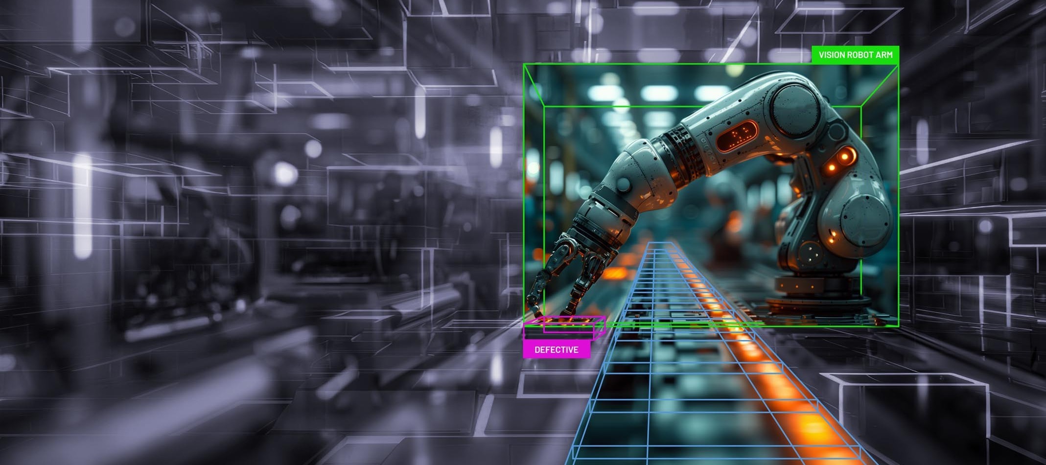
BlogAug 19, 2024
Challenges and Opportunities of Machine Learning in Quality Control
Manuel Botija | Head of Product at AXELERA AI Quality control and defect inspection are vital processes in manufacturing, ensuring that products meet stringent standards and are free from defects. AI-driven vision inspection systems (integral to quality control 4.0) have revolutionized these processes, providing high accuracy and efficiency in identifying defects that human inspectors might miss. These vision inspection systems use advanced imaging technologies and machine learning algorithms to automatically detect and classify defects, ensuring consistent quality across various industries.Discover how vision inspection system manufacturers can tackle the challenges associated with applying machine learning in quality control.Choosing the right AI-based algorithms Adapting to the uniqueness of each manufacturing line Deploying fast and secure inference, anywhere Scaling up and keeping upExample applications of vision inspection systemsAutomotive Industry: In the automotive sector, vision-based systems are used to inspect components such as engine parts, brake systems, and body panels. These systems utilize high-resolution cameras and image processing algorithms to detect defects like cracks, deformations, and surface irregularities that could compromise vehicle safety and performance. Electronics Manufacturing: Automated Optical Inspection (AOI) systems are widely used in the electronics industry to inspect printed circuit boards (PCBs). These systems capture high-resolution images of PCBs and use pattern recognition algorithms to identify defects such as missing components, soldering issues, and misalignments, ensuring that only functional electronics are shipped to customers. Textile Industry: Vision inspection systems in the textile industry scan fabrics to identify defects such as holes, stains, and color inconsistencies. These systems use cameras and image processing software to continuously monitor the fabric during production, ensuring high-quality textiles are produced without manual inspection. Food and Beverage Production: In the food and beverage industry, vision systems are used to inspect products for contamination and packaging defects. For example, x-ray and infrared imaging technologies can detect foreign objects in packaged foods, while high-speed cameras ensure that labels and seals are correctly applied. Pharmaceuticals: Vision inspection systems in the pharmaceutical industry ensure that tablets, capsules, and vials are free from defects. These systems use cameras and specialized lighting to inspect for cracks, chips, and discoloration, ensuring that only safe and effective medications reach consumers.These examples illustrate the significant role of vision inspection systems in enhancing product quality and safety across various manufacturing sectors. By leveraging advanced imaging and machine learning technologies, these systems provide manufacturers with reliable and efficient tools to maintain high standards and improve operational efficiency.Deep learning has changed quality control for the betterDeep learning has revolutionized defect inspection and quality control in manufacturing by providing unprecedented accuracy, speed, and adaptability. Traditional approaches that use hand-crafted algorithms on vision systems for manufacturing, while effective, have limitations in their ability to learn and adapt to new types of product defects and variations. Deep learning overcomes these limitations by leveraging vast amounts of data to train neural networks that can identify and classify defects with high precision.Deep learning models, particularly Convolutional Neural Networks (CNNs), have significantly improved the accuracy of defect detection. These models can automatically learn complex features from images, enabling them to detect even the smallest and most subtle defects. For instance, deep learning models can identify micro-cracks in semiconductor wafers, which are crucial for the electronics industry where even minor defects can lead to significant product failures. Thus, deep learning can significantly improve automated inspection.But the improvements of machine learning in quality control come with some challenges. Challenges and Opportunities of Machine learning in Quality Control1. Choosing the right AI-based algorithms for a given problemThe diversity of AI-based algorithms available for automated inspection pose a significant challenge for manufacturers. Different algorithms, based on classification, localization, and segmentation, apply to different problems. Choosing the right algorithm requires understanding the specific requirements of the defect recognition task at hand, which varies significantly across different manufacturing sectors.Classification algorithms allow identifying defects within a set of predefined classes (like classifying defective and non-defective microchips in the electronic industry) with CNN models such as ResNet which automatically learn and extract hierarchical features from images recognizing complex patterns Localization algorithms allow detecting the presence of defects within the image (like locating surface cracks on automotive parts). Models from the YOLO family can detect and localize multiple defects in real-time, making them suitable for high-speed manufacturing lines Segmentation algorithms precisely delineate the boundaries of defects within an image (for example segmenting defects on textile surfaces to identify the exact areas of flaws). U-Net is a popular CNN architecture for segmentation tasks. It excels whenever detailed localization of features within images is required thanks to its encoder-decoder structure that allows it to capture fine details and provide pixel-level segmentation. Anomaly detection identifies deviations from the norm without predefined defect classes (for example detecting unusual wear patterns on machinery parts that indicate potential failures). Variational Autoencoders (VAEs) are an example of an architecture used for anomaly detection. These models learn the normal distribution of the data and can identify anomalies as deviations from this distribution. VAEs, in particular, are used to model the normal appearance of components and flag deviations as defects.How Axelera AI addresses this challengeAt Axelera AI we know that our customers require a wide variety of models for their vision inspection systems. We address this challenge by offering a flexible and performant architecture designed to integrate and adapt to a wide variety of deep learning models at high resolution and high frame rates.Our unique In-Memory architecture is built with adaptability in mind, allowing seamless integration of new and emerging backbones (the part of neural networks that extract features from the input data, like ResNet and MobileNet). This helps us provide a comprehensive and ever-growing toolkit for defect inspection as part of our Model Zoo.Our Metis AI platform already supports a wide range of state-of-the-art models and features best-in-class performance across many models. This allows deploying real-time vision inspection systems with multiple high resolution, high frame rate cameras.2. Adapting to the uniqueness of each manufacturing lineThe fragmentation of problems across different manufacturing lines presents a significant challenge in automated inspection. Each line has unique requirements, materials, and processes, making it difficult to find a one-size-fits-all solution. Consequently, there is a need to adapt models specifically to each problem, often with limited data available for training. Here are the main approaches to solving this challenge:Retraining: Involves training a pre-existing model on new data specific to the manufacturing line. This process can be time-consuming and data-intensive but ensures that the model is tailored to the specific defects and characteristics of the production line. Fine-Tuning: Is a less resource-intensive method where a pre-trained model is slightly adjusted using a smaller, task-specific dataset. This approach is particularly useful when the available data is limited. Model-Agnostic Meta-Learning (MAML): Is a meta-learning technique where a model is trained on a variety of tasks such that it can quickly adapt to new tasks with minimal data. This approach is beneficial in environments where new types of defects may frequently arise. Zero-Shot Learning: Allows a model to recognize defects it has never seen before by leveraging knowledge from similar tasks or utilizing descriptive labels. This method is highly advantageous in scenarios with very limited or no defect data. How Axelera AI addresses this challengeAxelera AI addresses the challenge of adapting models for machine learning in quality control to the uniqueness of each manufacturing line by providing a robust and flexible solution that minimizes complexity. Our technology does not get in the way of training. Models that have been trained in a hardware-agnostic fashion can be compiled and run on our inference hardware seamlessly and without degradation in accuracy. We provide quantization libraries that automatically handle the optimization of models post-training. This enables efficient deployment without compromising performance and ensures that manufacturers can quickly implement tailored AI solutions to address specific defect inspection needs.3. Deploying fast and secure inference, anywhereDeploying AI models that enhance vision systems for manufacturing involves several critical challenges. Axelera AI makes sure they are addressed in order to ensure operational efficiency, privacy, and confidentiality. Manufacturing environments often consist of diverse hardware systems from various vendors running different operating systems. A manufacturing line might use a mix of Windows, Linux, and custom real-time operating systems across different machines from vendors like Dell, HP, and Lenovo. Axelera AI’s acceleration platform Metis is available as PCIe or M.2 modules and can be integrated into many hardware solutions, supporting a wide range of operating systems. This ensures compatibility with existing heterogeneous hardware setups. Manufacturing systems often have pre-existing software architectures that may be custom-built or rely on widely used libraries like GStreamer. Integrating AI models into these architectures without disrupting existing workflows and processes is achieved thanks to Axelera AI’s Voyager SDK. This SDK provides both low-level APIs and pipelines based on popular frameworks like GStreamer, allowing for easy integration into pre-existing software architectures. This flexibility ensures that AI models can be deployed without significant modifications to existing systems. AI inference needs to have low latency and high pixel throughput to meet the demands of real-time defect detection. This is especially important when multiple high-resolution cameras are used, or when the manufacturing process operates at high frames per second (fps). Metis delivers datacenter-grade performance at the edge, ensuring low latency and high throughput necessary for real-time defect detection. This capability is crucial for maintaining operational efficiency in high-speed manufacturing lines with multiple high-resolution cameras. Manufacturing data often includes sensitive information that cannot leave the premises due to privacy and confidentiality concerns. Axelera AI’s on-premises AI solution, addresses confidentiality and privacy concerns by ensuring that all data processing occurs within the manufacturing facility.
Related products:Industry
BlogJul 10, 2024
How Our Quantization Methods Make the Metis AIPU Highly Efficient and Accurate
Bram Verhoef | Director of Customer Engineering & Success at AXELERA AI To create a high-performing and highly energy efficient AI processing unit (AIPU) that obsoletes extensive model retraining, our engineers took a radically different approach to data processing. Through unique quantization methods and a proprietary system architecture, Axelera is able to offer the most powerful AI accelerator for the edge you can buy today. In this blog, you can read all about our unique quantization techniques.Industry-leading performance and usabilityOur Metis acceleration hardware leads the industry, because of our unique combination of advanced technologies. This is how our sophisticated quantization flow methodology enables Metis’ high performance and efficiency.Metis is very user-friendly, not in the least because of the quantization techniques that are applied. Axelera AI uses Post-Training-Quantization (PTQ) techniques. These quantization techniques do not require the user to perform any retraining of the model, which would be time-, compute- and cost-intensive. Instead, PTQ can be performed quickly, automatically, and with very little data. Metis is also fast, energy-efficient and cost-effective. This is the result of innovative hardware design, like digital in-memory-computation and RISC-V, but also from the efficiency of the algorithms running on it. Our efficient digital in-memory-computation works hand in hand with quantization of the AI algorithms. The quantization process casts the numerical format of the AI algorithm elements into a more efficient format, compatible with Metis. For this, Axelera AI has developed an accurate, fast and easy-to-use quantization technique.Model Deviation from FP32 accuracy ResNet-34 -0.1% ResNet-50v1.5 -0.1% SSD-MobileNetV1 -0.3% YoloV5s-ReLu -0.9% Accuracy drop @ INT8 Highly accurate quantization techniqueIn combination with the mixed–precision arithmetic of the Axelera Metis AIPU, our AI accelerators can deliver an accuracy practically indistinguishable from a reference 32-bit floating point model. As an example, Metis AIPU can run the ResNet50v1.5 neural network processing, at a full processing speed of 3,200 frames per second, with a relative accuracy of 99.9%. Technical details of our post-training quantization methodTo reach high performance, AI accelerators often deploy 8-bit integer processing of the most compute-intensive parts of neural network calculations instead of using 32-bit floating-point arithmetic. To do so, a quantization of the data from 32-bit to 8-bit needs to be done.The Post-Training Quantization (PTQ) technique begins with the user providing around hundred images. These images are processed through the full-precision model while detailed statistics are collected. Once this process is complete, the gathered statistics are used to compute quantization parameters, which are then applied to quantize the weights and activations to INT8 and other precisions in both hardware and software.Additionally, the quantization technique modifies the compute graph to enhance quantization accuracy. This may involve operator folding and fusion, as well as reordering graph nodes. Our radically different approach to data processingFrom the outset, we designed our quantization method with two primary goals in mind. The first goal is achieving high efficiency, the second is high accuracy. Our quantized models typically maintain accuracy comparable to full-precision models.To ensure this high accuracy, we begin with a comprehensive understanding of our hardware, as the quantization techniques employed depend on the specific hardware in use. Additionally, we utilize various statistical and graph optimization techniques, many of which were developed in-house. Compatible with Various Neural NetworksBy employing a generic quantization flow methodology, our systems can be applied to a wide variety of neural networks while minimizing accuracy loss.Our quantization scheme and hardware allow developers to efficiently deploy an extremely wide variety of operators. This means that Axelera AI's hardware and quantization methods can support many different types of neural network architectures and applications.
Related products:AI Accelerators
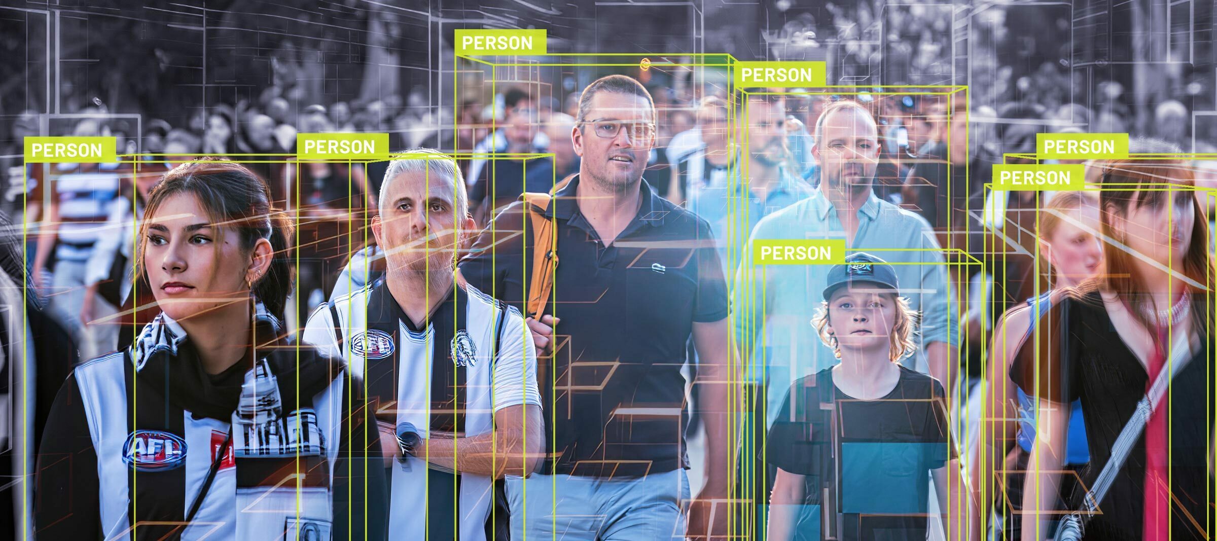
BlogApr 23, 2024
AI Access Control: How to Accelerate Verification Without Sacrificing Accuracy
Access control is a fundamental element in safeguarding both physical and digital environments. Integrating vision AI has significantly advanced access control systems, offering a level of automation and intelligence previously unattainable. Especially for biometric access control systems. Yet, the challenge remains: How can we speed up verification without compromising accuracy? More specifically, how do we reduce false positives and negatives?This blog explores the current and future state of AI access control, the pivotal role of verification speed, and a method to increase verification speed without increasing false positives in security. The Evolution of Vision AI in Access ControlAt present, vision AI applications in (biometric) access control systems are primarily used for identification and verification, and sometimes for motion detection and behavior analysis. With technologies like facial recognition, object detection and anomaly detection, we've moved from reactive to proactive security measures. Looking ahead, we envision a more sophisticated integration of AI in access control, where adaptive learning algorithms can predict potential security breaches before they occur, and personalized access protocols cater to the unique security requirements of individual users or entities.The Critical Importance of Speed in VerificationIn today’s fast-paced world, rapid verification in access control is not just a convenience; it's a necessity. Delays in access verification can lead to bottlenecks in high-traffic environments, disrupt operations, and degrade the user experience. More critically, the speed at which individuals can be verified and granted access can be a matter of life and death.Low speed of processing and available performance headroom of the equipment used may increase the risk of missing detection of people or objects due to an inability to use more advanced and more reliable image processing, such as using the latest neural networks, such as YOLOv8, picking the best picture from several, alignment, and real-time matching. Why Accuracy Matters TooEvery millisecond saved in the verification process enhances the user experience and operational efficiency. However, every incorrect decision made by the system — be it a false positive or a false negative — undermines trust in the security framework and can cause delays itself. High traffic environments, such as airports, commercial buildings, and public events, require a solution that combines high-speed, high-accuracy verification to maintain security without disrupting the flow of movement. The goal, therefore, is a verification process that is not only fast but also reduces false positives and false negatives in security to the absolute minimum.The Challenge with Current AI AcceleratorsCurrent AI accelerators have made significant strides in improving the efficiency of running vision AI models. However, they often face a trade-off between speed and accuracy, as they commonly deploy 8-bit integer inference arithmetic instead of 32-bit floating-point full-precision. High verification speeds can sometimes result in increased false positives and negatives, as the security and surveillance systems may not spend enough time analyzing the data to make accurate decisions. This is particularly problematic in access control, where errors can either compromise security by allowing unauthorized access or hinder operations by denying access to legitimate users. Therefore, eliminating false negatives and false positives in machine learning used for automatic identification is important.Fortunately, Axelera AI solved the challenge of reducing precision of the mathematical computations without any practical accuracy loss, eliminating the false positives in security processes produced by vision AI accelerators. The exceptional performance and accuracy of the Axelera AI acceleration platform have significantly fueled our collaborative efforts. Its unmatched performance-to-price ratio, surpassing traditional GPUs and dedicated AI processing units, has been critical in our selection process. We are confident that leveraging their state-of-the-art YOLO performances will empower us to tackle new challenges in our current and future video analysis applications.Alexandre Perez, R&D Director at XXII. How We Accelerated Vision AI Applications Without Accuracy LossTo address the challenges outlined above, our engineers took a radically different approach to data processing. By combining Axelera’s proprietary digital in-memory computing technology (D-IMC) and a unique post-quantization method, Axelera has created the Metis AIPU – the most powerful AI accelerator for the edge you can buy today. Its unmatched efficiency and accuracy redefine the standard for AI access control. The technology ensures that vision AI models run with the same accuracy as PCs or GPUs (FP32 equivalent), but at significantly lower cost and power consumption while delivering the highest level of accuracy to minimize false positives and negatives. It can make biometric access control systems not only efficient but also highly reliable.
Related products:Industry

Jan 22, 2024
Davos 2024: AI's Evolution and the Edge Revolution
Bram Verhoef | Director of Customer Engineering & Success at AXELERA AI At this year’s World Economic Forum in Davos, the spotlight was firmly placed on artificial intelligence (AI), reflecting its growing importance across various sectors. The discussions not only highlighted AI’s expansive role but also emphasized the evolving trend of edge computing driven by specialized hardware accelerators.The topic captivated the forum for several days due to its impact on scaling AI applications, the accelerating pace of technological advancements, and the democratization of AI through open-source models. Among the people that were at the center of the debate and on stage discussions were Yann LeCun, Kai-Fu Lee, Daphne Koller, Andrew Ng, and Aidan Gomez that contributed deep insights into the potential and direction of AI growth.Here are some deeper insights into these topics, offering a glimpse into the future shaped by AI and edge computing. AI’s Ubiquity in Davos Discussions AI dominated discussions in Davos, underscoring its critical role in both posing challenges and offering solutions. This ranged from ethical considerations and privacy concerns to AI’s potential in enhancing safety and efficiency in industries such as surveillance, healthcare, finance, and manufacturing. Strategic Imperative of AI Adoption There was a consensus on the need for comprehensive AI strategies within the next five years. This goes beyond merely adopting AI technologies; it involves integrating AI into core business processes, understanding its impact on customer engagement, and rethinking how AI can drive innovation and competitive advantage. AI as a Collaborative Partner AI was widely recognized as a collaborator that augments human capabilities. This concept extends to various sectors, from creative industries using AI for design and content generation to legal and medical fields where AI assists in analysis and diagnostics, enhancing the expertise of professionals. The Need for AI Fluency A recurring theme was the importance of AI literacy in the workforce. This means not just understanding AI but being adept at leveraging AI tools for decision-making, problem-solving, and innovation. It highlights the need for continuous learning and upskilling in the age of AI. AI and Productivity: A Symbiotic Relationship Discussions also focused on AI’s role in boosting productivity, especially in the context of aging populations and slower economic growth. AI’s ability to automate complex tasks and analyze large data sets can drive efficiency, leading to job creation in AI development, management, and maintenance. AI as a Catalyst for Scientific Discovery AI’s potential to revolutionize scientific research was a prominent topic. From drug discovery and climate modeling to exploring new materials, AI’s ability to process vast amounts of data and identify patterns can significantly accelerate scientific breakthroughs. The Open Source AI Debate The role of open-source AI was acknowledged as vital in democratizing access to AI technologies. However, concerns were raised about the safety and ethical use of AI, emphasizing the need for robust governance frameworks to manage these open-source resources responsibly. AGI: A Work in Progress Artificial General Intelligence (AGI) was discussed as an emerging yet influential area. While current AI systems excel in specific tasks, the pursuit of AGI aims at creating more versatile, human-like intelligence, marking a significant leap in AI capabilities. Artificial General Intelligence (AGI) was discussed as an emerging area. While today’s AI systems exhibit increasing levels of generality, there is a clear need for further advancement to enhance their overall applicability. Despite the growing sophistication of AI, it notably lacks certain core aspects intrinsic to human intelligence. Key among these are the abilities to learn from a limited number of examples and to achieve visual grounding. Intriguingly, these areas are currently at the forefront of AI research, sparking considerable interest and anticipation for significant progress in the coming year. Tailored AI While 2023 was the year of general large language models, 2024 will be the year of customized experienced. For consumers, OpenAI has just released the AI store with millions of customized models to serve specific purposed. In the business-to-business market companies will start deploying custom models, tailored on specific applications and fine-tuned with proprietary data, preserving privacy, security and intellectual proprieties. AI at the Edge: The Future of Digital Interactions A key foresight from Davos was the move towards processing data at the edge, in proximity of the user, facilitated by hardware accelerators. This approach is crucial for real-time processing and response, essential for applications ranging from industrial 4.0, autonomous vehicles to smart cities, where delay in data processing can have critical implications. The Axelera AI RevolutionAs Europe’s largest player in the AI acceleration space, we are pioneering this shift towards edge-centric AI. Our focus on developing cutting-edge hardware accelerators is pivotal in bringing the power of AI closer to where data is generated, reducing latency, enforcing data privacy, and enhancing efficiency. This is not just about advancing technology; it’s about reshaping how we interact with and benefit from AI in our daily lives. As we lead this charge, Axelera AI remains committed to innovating and driving forward a future where AI is more accessible, efficient, and integrated into the fabric of our evolving digital world.
Related products:Company
Filter by Type
- Everything
- AI Accelerators
- AI Software
- Company
- Evaluation Systems
- Industry
- Technology
- Axelera Community
Sign up
Already have an account? Login
Log in, or create an Axelera AI account
Log In or Register HereEnter your E-mail address. We'll send you an e-mail with instructions to reset your password.
Scanning file for viruses.
Sorry, we're still checking this file's contents to make sure it's safe to download. Please try again in a few minutes.
OKThis file cannot be downloaded
Sorry, our virus scanner detected that this file isn't safe to download.
OK